Method for independently regulating and controlling spin orbit coupling parameters of semiconductor quantum well

A technology of spin-orbit coupling and quantum well, which is applied in the direction of semiconductor devices, single semiconductor device testing, electrical measurement, etc., can solve the problems of discontinuous regulation, complicated problems, unfavorable quantitative analysis, etc., and achieve remarkable regulation effect and feasibility high effect

Inactive Publication Date: 2020-05-29
JILIN UNIV
View PDF10 Cites 1 Cited by
  • Summary
  • Abstract
  • Description
  • Claims
  • Application Information

AI Technical Summary

Problems solved by technology

[0003] So far, people have made many attempts to control the spin-orbit coupling of semiconductor quantum wells: using the energy valley phase transition caused by the electric field-induced carrier distribution of GaAs can realize the electric field control of the spin-orbit coupling: but the control is discontinuous And it is difficult to achieve in other materials, and it is not universal; use the ratio adjustment of elements in the alloy to change the spin-orbit coupling of the material: but this regulation is not performed in situ and the prepared samples are introduced due to different components Defects and impurities, which complicate the problem and are not conducive to quantitative analysis; changing the quantum well width is an effective method to independently adjust the parameters of the Dresselhaus spin-orbit coupling: but this method needs to prepare different quantum well samples, the cost is high and the original method cannot be carried out. Bit regulation; Rashba and Dresselhaus spin-orbit coupli

Method used


Image

  • Method for independently regulating and controlling spin orbit coupling parameters of semiconductor quantum well
  • Method for independently regulating and controlling spin orbit coupling parameters of semiconductor quantum well
  • Method for independently regulating and controlling spin orbit coupling parameters of semiconductor quantum well

Examples


Embodiment 1

[0026] Embodiment 1 Overall process of the present invention

[0027] The overall technical solution of the present invention will be specifically described below in conjunction with the accompanying drawings. The invention is a method for independently regulating the Rashba and Dresselhaus spin-orbit coupling strength parameters of semiconductor quantum wells. By changing the pressure and gate voltage of the sample at the same time, the independent regulation of the InSb quantum well Rashba and Dresselhaus spin-orbit coupling strength parameters α and γ can be realized, specifically including the following steps,

[0028] Step S1: Select a semiconductor quantum well sample with asymmetric doping and a controllable metal gate;

[0029] Step S2: Put the sample in the step S1 into the piston-sleeve type electrical measurement high-pressure chamber, and apply pressure and grid voltage to the sample;

[0030] Step S3: The Rashba and Dresselhaus spin-orbit coupling parameters are...

Embodiment 2

[0031] The concrete implementation of embodiment 2 step S1

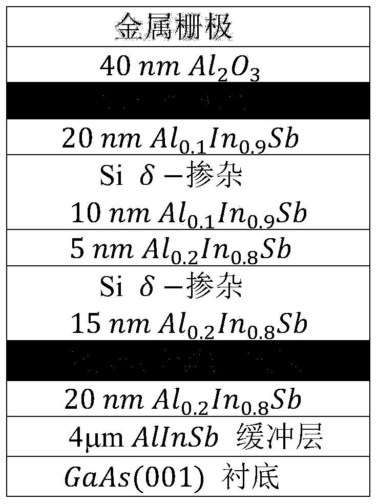
[0032] The sample selected in step S1 is an InSb quantum well, and its layered structure schematic diagram is as follows figure 1 As shown, from bottom to top is (001) plane semi-insulating GaAs substrate, 4 micron (μm) Al 0.1 In 0.9 Sb and Al 0.2 In 0.8 Alternately grown buffer layers of Sb, 20 nanometers (nm) of Al 0.2 In 0.8 Sb barrier layer, 20nm InSb quantum well, 15nm Al 0.2 In 0.8 Sb barrier layer, Siδ-doped, 5nm Al 0.2 In 0.8 Sb barrier layer, 10nm Al 0.1 In 0.9 Sb barrier layer, Siδ-doped, 20nm Al 0.1 In 0.9 Sb barrier layer, 10nm InSb surface layer, 40nm Al2O3 insulating layer, metal gate. Step S1 specifically includes the following steps:

[0033] Step S11: grow an InSb quantum well sample on the (001) plane GaAs substrate by molecular beam epitaxy, the growth process of the sample is as follows: first grow a 4 μm thick Al on the GaAs substrate 0.1 In 0.9 Sb and Al 0.2 In 0.8 Sb buffer la...

Embodiment 3

[0036] The specific implementation of embodiment 3 step S2

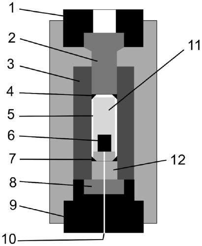
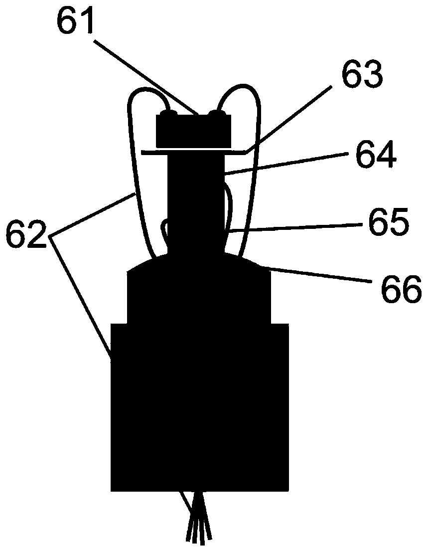
[0037] The schematic diagram of the structure of the piston-sleeve type electric measuring high pressure chamber used in the step S2 is as follows: figure 2 As shown, 1 is the pressure bolt, 2 is the pressure piston, 3 is the press sleeve, 4 is the upper sealing gasket, 5 is the Teflon pressure chamber, 6 is the quantum well sample and corresponding components, 7 is the lower sealing gasket, 8 9 is a bottom support bolt, 10 is a lead through hole, 11 is a pressure transmission medium, and 12 is a lead through column. Wherein, quantum well samples and corresponding components 6 such as image 3 shown in image 3 Among them, 61 is a semiconductor quantum well device, 62 is a wire, 63 is a sample support plate, 64 is a light-emitting diode, 65 is a conductive silver glue, and 66 is a sealant. Step S2 specifically includes the following steps:

[0038] Step S21: Load the quantum well sample and light-emitting diodes...


PUM


Abstract

The invention discloses a method for independently regulating and controlling spin orbit coupling parameters of a semiconductor quantum well and belongs to the technical field of semiconductor spintronics. The method comprises steps of selecting an asymmetrically doped semiconductor quantum well sample with a controllable metal gate; loading the sample into a piston sleeve type electric measurement high-voltage cavity, and applying pressure and a gate voltage to the sample; acquiring rashba and Dresselhaus spin orbit coupling parameters through anti-weak localization measurement, and realizingindependent regulation and control of the two spin orbit coupling parameters by adjusting the pressure and the grid voltage at the same time. The method for regulating and controlling the spin orbitcoupling strength parameters of the semiconductor quantum well is high in feasibility and can be carried out in situ, a new sample does not need to be prepared, independent regulation and control of the two parameters can be achieved respectively, and the regulation and control effect is remarkable.

Description

technical field [0001] The invention belongs to the technical field of semiconductor spin electronics, and in particular relates to a method for independently regulating the Rashba and Dresselhaus spin-orbit coupling parameters of semiconductor quantum wells. Background technique [0002] With the development of spintronics, the study of electron spin characteristics has become the most popular research direction in the field of condensed matter physics. The spin-orbit coupling with relativistic effect can closely link the spin and orbital motion of electrons, and then the spin-orbit coupling can be used to realize the full electrical control of electron spin and to prepare spin field effect transistors and qubits. The spin-orbit coupling interaction in the quantum well composed of semiconductor compounds is mainly composed of two parts: one is the Dresselhauss effect caused by the lack of bulk inversion symmetry center in the material, which includes two parts of the linear...

Claims


Application Information

Patent Timeline
IPC IPC(8): G01R31/26H01L29/66
CPCG01R31/2601H01L29/66984
Inventor 杨凯锋李恒梅刘洪武
Owner JILIN UNIV
Why Eureka
Try Eureka