Unsupported, electron transparent films and related methods

a technology of electron transparent film and electron beam, which is applied in the direction of liquid/fluent solid measurement, instruments, machines/engines, etc., can solve the problems of time-consuming and destructive, no ordinary surface of any practical thickness is transparent, and the procedure requires careful and tedious attention

Inactive Publication Date: 2008-03-25
UNIV OF WASHINGTON
View PDF5 Cites 15 Cited by
  • Summary
  • Abstract
  • Description
  • Claims
  • Application Information

AI Technical Summary

Problems solved by technology

No ordinary surface of any practical thickness is transparent enough to electrons to allow immediate viewing in the microscope.
Sample preparation procedures vary dramatically from sample to sample, and virtually all are time-consuming and destructive, typically requiring significant time to acquire the requisite skill.
Although the conventional technique for making metallic films for TEM has been around for some time, the procedure requires careful and tedious attention, making the procedure a highly labor-intensive process available in studies where only a limited number of surfaces are necessary for study.
This process generally requires films too thick for good electron transparency and suffers from poor yields.

Method used


Image

  • Unsupported, electron transparent films and related methods
  • Unsupported, electron transparent films and related methods
  • Unsupported, electron transparent films and related methods

Examples


Embodiment Construction

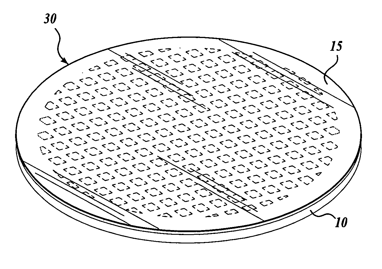
[0019]In one aspect, the invention provides unsupported, electron transparent films. The films are ultrathin, electron transparent, stable under an electron beam, and useful in electron microscopy and spectroscopy. In certain embodiments, the films of the invention are metal films. The metal films of the invention are alternatives to commercially available carbon-and silicon-based films.

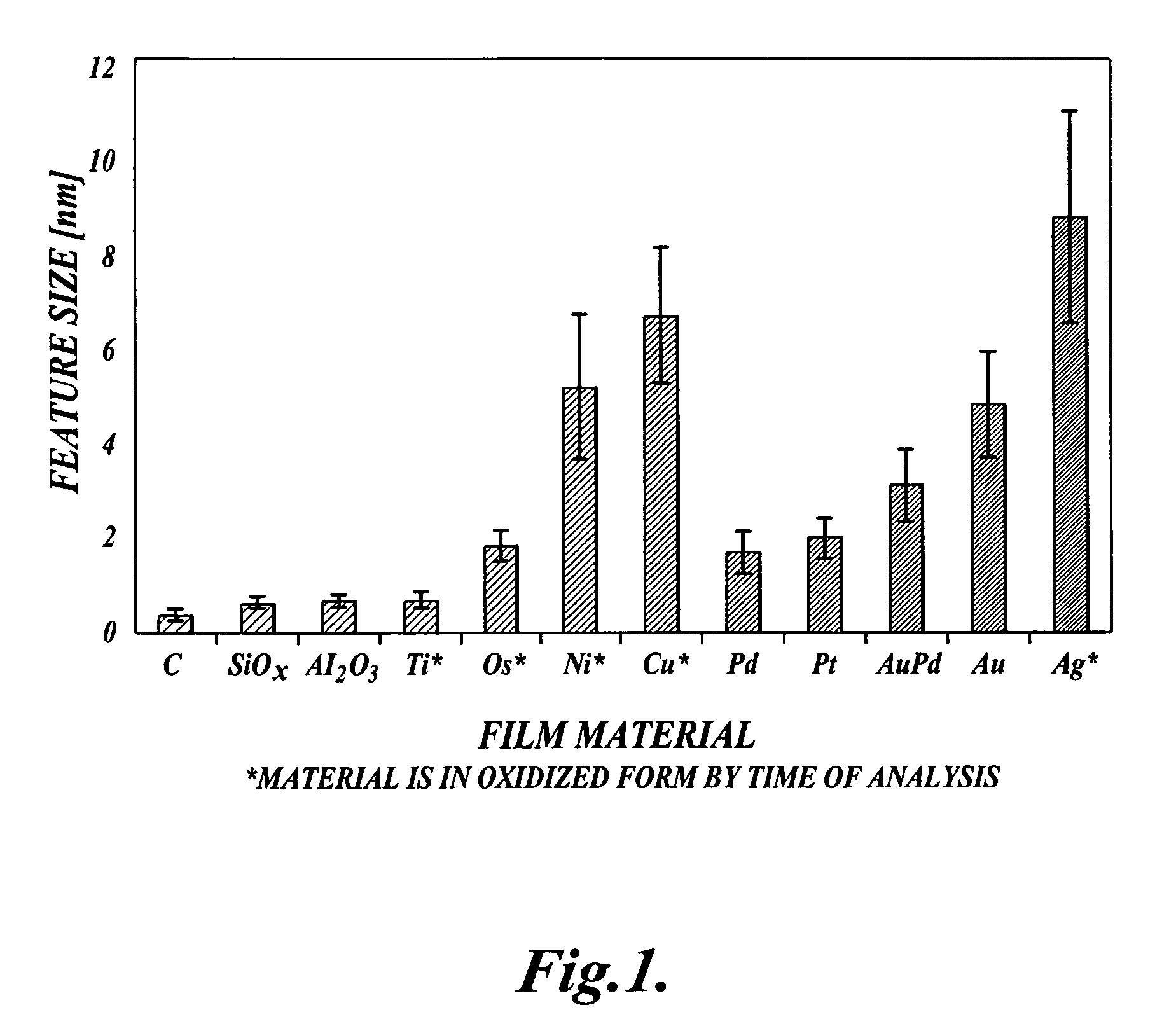
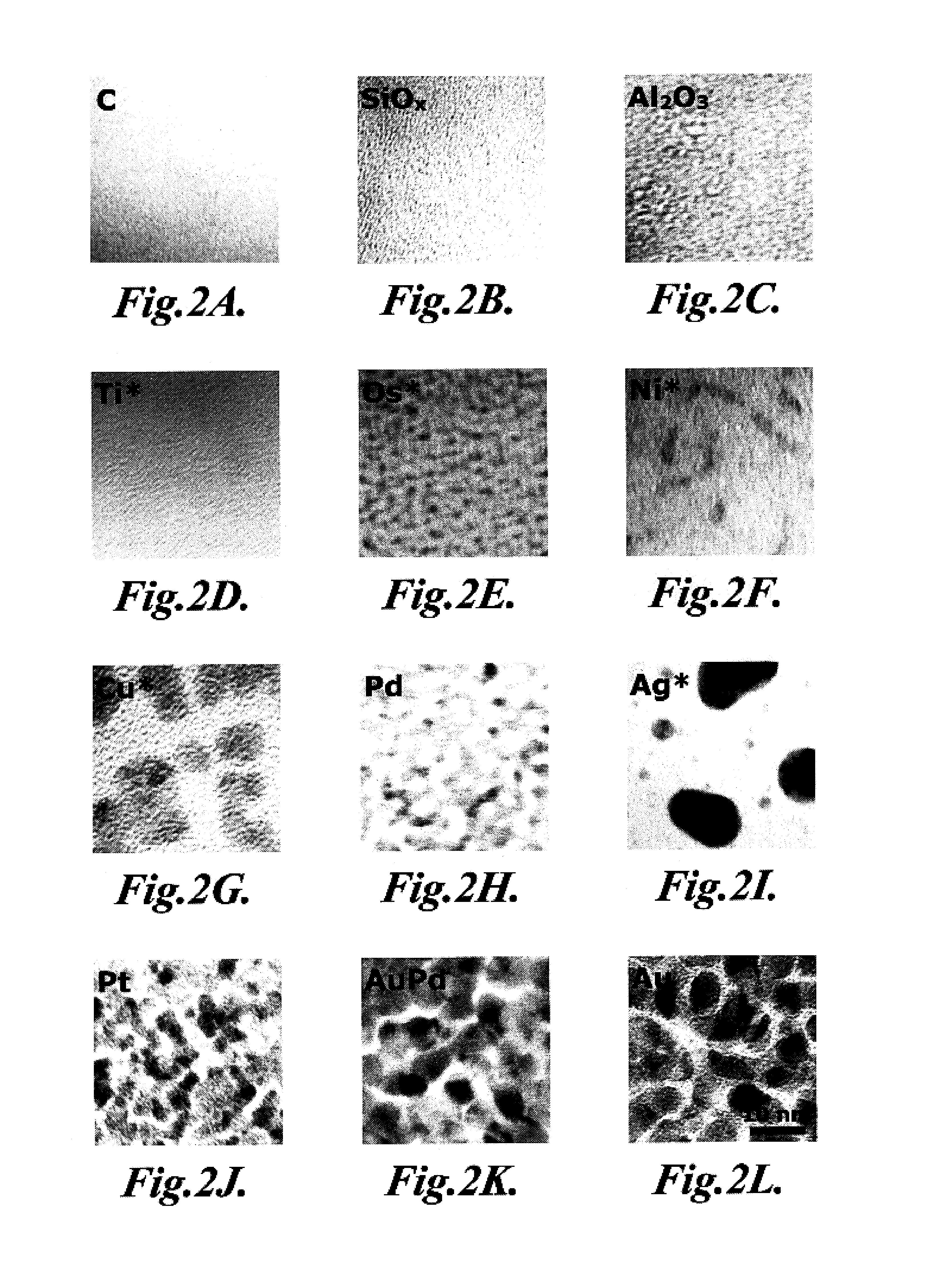
[0020]In certain embodiments, the films of the invention are made of one of a variety of metals, metal alloys, metal oxides, and combinations thereof. Suitable metals, alloys, and oxides include gold, silver, copper, nickel, titanium, palladium, platinum, iridium, rhenium, ruthenium, osmium, or rhodium, their alloys and oxides. In one embodiment, the metal film is made from one or more noble metals. Such a film may be useful in surface science applications. In one embodiment, the metal film is made from one or more semiconductor materials such as gallium arsenide. In one embodiment, the metal film is...


PUM

PropertyMeasurementUnit
thicknessaaaaaaaaaa
thicknessesaaaaaaaaaa
thicknessaaaaaaaaaa

Abstract

Unsupported, electron transparent film useful in supporting a sample for imaging and analysis by transmission electron microscopy; methods for making and using the unsupported, electron transparent film; and an integrally formed combination of an unsupported, electron transparent film and substrate.

Description

STATEMENT OF GOVERNMENT LICENSE RIGHTS[0001]This invention was made with government support under grant DAAD19-01-0499 awarded by the United States Army Research Office. The government has certain rights in the invention.FIELD OF THE INVENTION[0002]The present invention relates to unsupported, electron transparent films and methods for making and using unsupported, electron transparent films.BACKGROUND OF THE INVENTION[0003]Metal surfaces are known for their very high surface energies and interesting chemistry. In modem integrated circuit microfabrication technology, thin metal films are deposited as seed layers for adhesion and electrical continuity for electroplating processes. In various surface science and microbiology applications, noble metals are useful as completely inert background surfaces that can be chemically coupled with alkanethiol-derived molecules. In the various forms of oxides, sulfides, and selenides, metals make interesting compound semiconductors that are the s...

Claims


Application Information

Patent Timeline
Patent Type & Authority Patents(United States)
IPC IPC(8): H01J37/20B32B3/10
CPCH01J37/20Y10T428/24331H01J2237/262H01J2237/26
Inventor ALLRED, JR., DANIEL BSCHWARTZ, DANIEL T
Owner UNIV OF WASHINGTON
Why Eureka
Try Eureka