Test structures and models for estimating the yield impact of dishing and/or voids

a technology of test structures and models, applied in individual semiconductor device testing, semiconductor/solid-state device testing/measurement, instruments, etc., can solve problems such as malfunction of affected chips, electricly measurable faults (killer defects), and particularly significant topography-related defects

Inactive Publication Date: 2008-03-25
PDF SOLUTIONS INC
View PDF15 Cites 13 Cited by
  • Summary
  • Abstract
  • Description
  • Claims
  • Application Information

AI Technical Summary

Problems solved by technology

Defects (e.g., residual extra material) can cause electrically measurable faults (killer defects), depending on the chip layout as well as the layer and location of the defects.
These faults are responsible for manufacturing-related malfunction of affected chips.
Topography-related defects are particularly significant in the copper Damascene manufacturing method.
These variations result in non-uniform layer thicknesses (i.e., topography) within the final patterns of each chip as well as chip-to-chip across wafers and lots.
Since most chips have several layers of Cu metallization or other metallization, these thickness variations can further accumulate in each successive layer of processing resulting in complex overall topographical variations.
The usual countermeasure in this situation is to increase the CMP removal rate to achieve sufficient “overpolish.” However, too much overpolish can actually remove too much of the Cu metal in a given pattern, resulting in excessive metal resistance or a “missing material” defect.
Residual barrier metal defects are difficult to detect even using optimized inline inspection.
If an extra material defect occurs between the two halves of the comb 203, 204, the resulting electrical short results in excessive leakage current detected during subsequent electrical test.

Method used


Image

  • Test structures and models for estimating the yield impact of dishing and/or voids
  • Test structures and models for estimating the yield impact of dishing and/or voids
  • Test structures and models for estimating the yield impact of dishing and/or voids

Examples


Embodiment Construction

[0027]U.S. Provisional Patent Application No. 60 / 316,317, filed Aug. 31, 2001, is incorporated by reference herein in its entirety.

[0028]Introduction

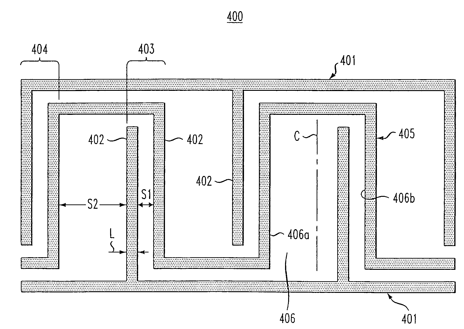
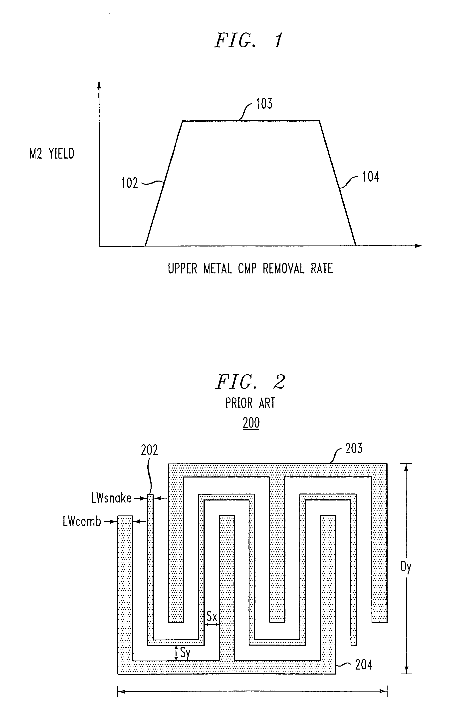
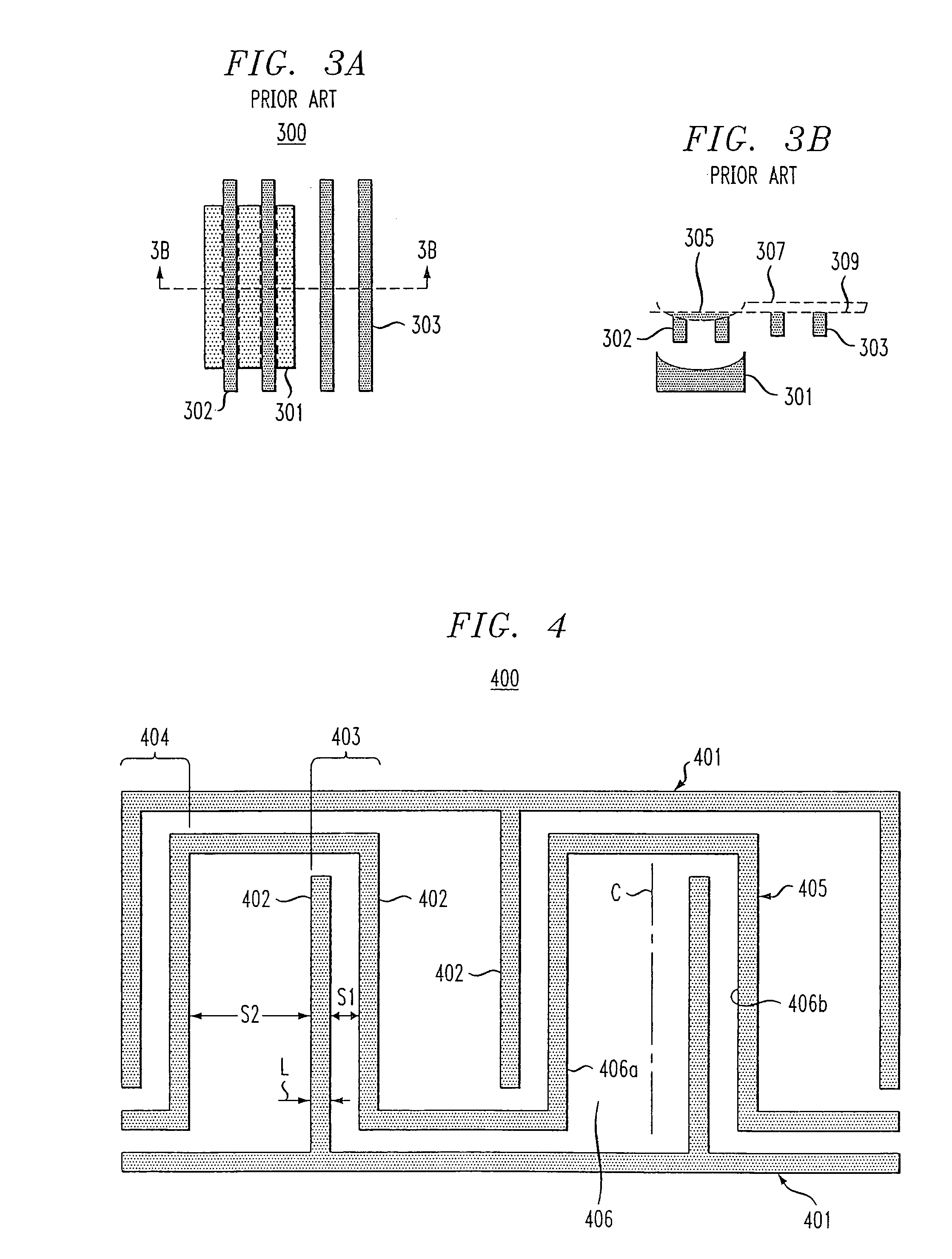
[0029]Cu (or other material) dishing on lower metal layers is known to cause residual barrier metal material on the next metal layer resulting in electrical shorts. Oxide dishing and metal void formation in the lower metal layers have also been observed to lead to electrical shorts in upper metal layers. The probability of these types of failure depends on several factors:[0030]1. the probability of Cu (or other metal) dishing, oxide dishing or Cu (or other metal) voiding in the lower metal layer[0031]2. the probability of transfer of lower layer topography into upper layer oxide topography

[0032]3. the removal rate during the final polishing step during upper metal layer formation

[0033]4. the presence of upper layer metal in close enough proximity to the residual material defect to result in a short in the upper layer metal.

[0034]Prior ...


PUM


Abstract

A test structure comprising a test pattern is formed on a substrate. The test pattern includes a first comb structure having a plurality of tines, and a second structure. The second structure may be a snake structure having a plurality of side walls or a second comb structure having a plurality of side walls. The tines of the first comb structure are positioned within side walls of the snake structure or second comb structure. The tines of the first comb structure are offset from a center of the side walls. Test data collected from the test structure are analyzed, to estimate product yield. The test structure may have a lower layer pattern, such that topographical variations of the lower layer pattern propagate to an upper layer pattern of the test structure.

Description

[0001]This application claims the benefit of U.S. Provisional Patent Application No. 60 / 316,317, filed Aug. 31, 2001.FIELD OF INVENTION[0002]This invention relates to methods for measuring and evaluating the process and design related statistical variations of an integrated circuit manufacturing process in order to determine their sources and their effects on the yield and performance of the product.BACKGROUND[0003]Defects (e.g., residual extra material) can cause electrically measurable faults (killer defects), depending on the chip layout as well as the layer and location of the defects. These faults are responsible for manufacturing-related malfunction of affected chips. So, a layer and fault sensitive defect density is important for yield enhancement and to control quality of process steps and product chips. See Staper, C. H., Rosner, R. J., Integrated Circuit Yield Management and Yield Analysis: Development and Implementation IEEE Transactions on Semiconductor Manufacturing, pp...

Claims


Application Information

Patent Timeline
Patent Type & Authority Patents(United States)
IPC IPC(8): H01L23/58H01L21/66H01L23/544
CPCH01L22/34
Inventor CIPLICKAS, DENNIS J.STINE, BRIAN E.FEI, YANWEN
Owner PDF SOLUTIONS INC
Why Eureka
Try Eureka