Universal measuring adapter system

a technology of adapter system and pin, applied in the direction of individual semiconductor device testing, measurement instrument housing, instruments, etc., can solve the problems of difficult economic viability of relatively small series of identical packages, incongruous pin assignment, and complex procedur

Inactive Publication Date: 2008-04-08
INFINEON TECH AG
View PDF10 Cites 8 Cited by
  • Summary
  • Abstract
  • Description
  • Claims
  • Application Information

AI Technical Summary

Benefits of technology

[0011]A package of which the semiconductor component is to be electrically measured is initially placed into the socket adapter and, adapted to such an extent, can be connected to the most varied devices, in particular probe stations, testers or curve tracers, and be operated, measured and / or analyzed there in the most varied of ways, without further complex and cost-intensive adaptations having to be performed.
[0014]The configuration of the adapter boards with plated-through holes and their connection to one another by means of plug-in contacts, each of the adapter boards being provided with redistribution routing in such a way that the distribution of the plug-in contacts of the socket is transformed into the standardized grid of the PGA socket, represents a favorable embodiment, since, along with the lower space requirement in comparison with contacting by means of contact areas, it is possible, according to the application in question, to produce both a detachable contact, by the plug-in connection, and a soldered plug-in connection, to increase the contact reliability.

Problems solved by technology

However, the assignment of the pins is not necessarily consistent, but depends on the type of components located in the package and also on the user-specific requirements.
The fact that the completed packages have to be subjected to a functional test, and possibly a burn-in (artificial pre-aging) prior to their delivery creates the problem that on the one hand a special socket (for example a burn-in socket) is required for each type of package and on the other hand a special tester board is necessary, allowing the electrically wired pins to be reliably contacted and connected to a testing device.
Such a procedure is very complex, however, and consequently cost-intensive, and is, therefore, scarcely economically viable for relatively small series of identical packages.

Method used


Image

  • Universal measuring adapter system
  • Universal measuring adapter system
  • Universal measuring adapter system

Examples


Embodiment Construction

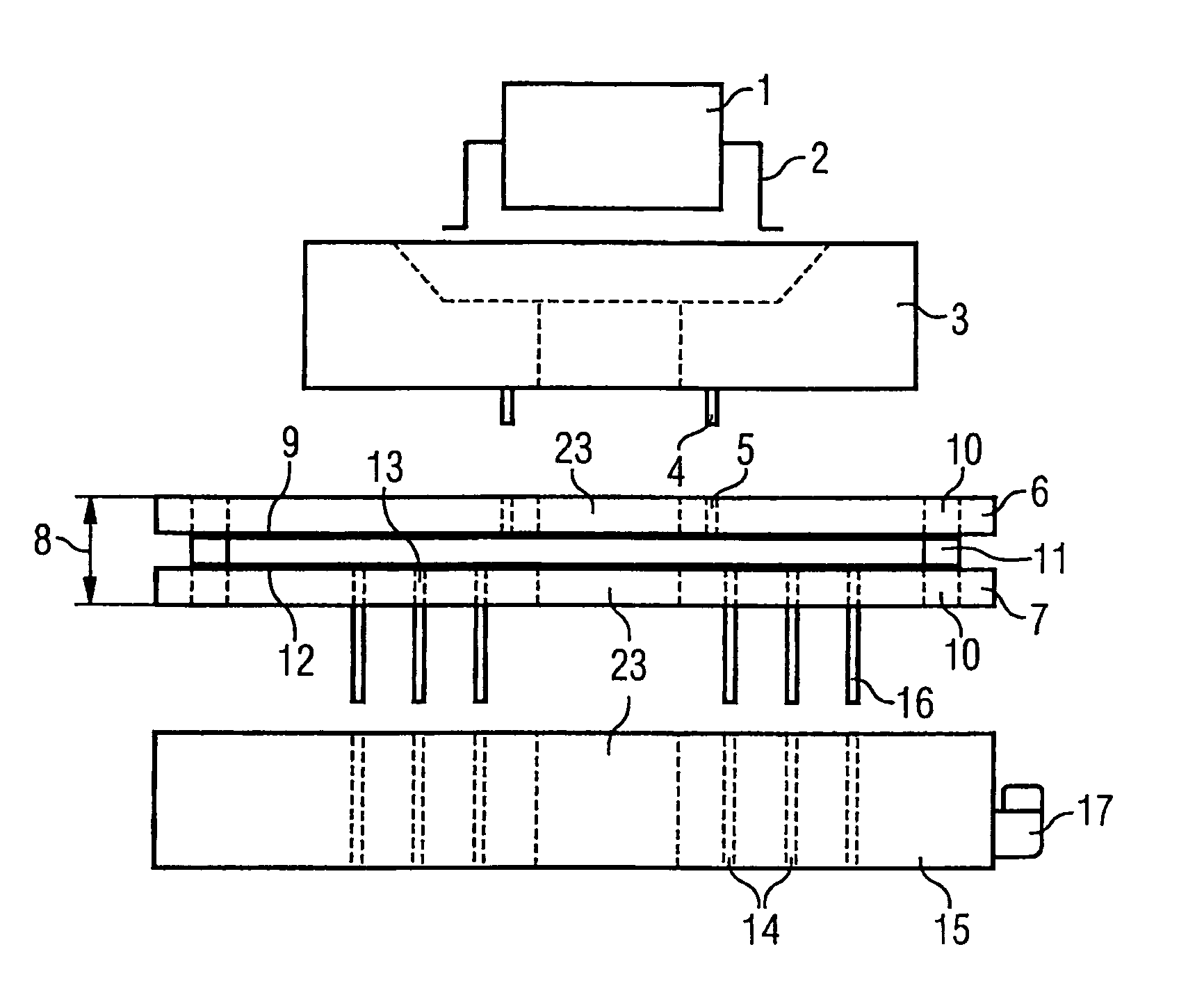
[0045]As represented in FIG. 1, the package 1 has laterally protruding pins 2, which are angled away twice in the downward direction to produce the contact with the socket 3. This socket 3 replicates 1:1 the terminal assignment of the pins 2 of the package 1 on first plug-in contacts 4 protruding on its underside.

[0046]These first plug-in contacts 4 are plugged into first plated-through holes 5 of the upper adapter board 6 of a system of two connected adapter boards, referred to hereafter as socket adapter 8, soldered and consequently electrically connected. The upper adapter board 6 has on its underside a first pattern of conductive traces 9, which redistributes the routing from the first plated-through holes 5 to second plated-through holes 11 in the outer region of the upper adapter board 6. By plugging together and subsequently soldering the second plug-in contacts 10 with the second plated-through holes 11, the latter being located in corresponding positions in the outer region...


PUM


Abstract

The invention relates to a universal measuring adapter system for adapting or contacting semiconductor components in the most varied packages for electrically operating and measuring the same. The pins or contact pads of the package are electrically contacted on the input side in a specially adapted socket, and the socket, on the side of the device (output side), has contact pins whose pin assignment corresponds to the pin assignment of the package contacted inside the socket. The aim of the invention is to create a universal measuring system for adapting or contacting semiconductor components in the most varied packages for electrically operating, measuring and analyzing the same, with which, on the side of the device, the pin numbers can always be tapped at the same location regardless of the package and which is suited for expansion stages with any number of pins and pin configurations. To this end, a socket adapter, which is comprised of at least one adapter board, is arranged between the socket and a PGA socket with a standardized contact assignment. Said socket adapter depicts the rewiring of each individual connection of the package in a special pattern that always has the same orientation.

Description

[0001]This application is a continuation of co-pending International Application No. PCT / DE2003 / 004176, filed Dec. 18, 2003, which designated the United States and was not published in English, and which is based on German Patent Application No. 103 01 124.2 filed Jan. 14, 2003, both of which applications are incorporated herein by reference.TECHNICAL FIELD[0002]The invention relates to a universal measuring system for adapting or contacting semiconductor components in the most varied packages for electrically operating, measuring and analyzing the same, in which system the packages are electrically contacted in a specially adapted socket.BACKGROUND[0003]In practice, the most varied packages for semiconductor components are developed and used according to the application requirements, it being possible for the number of pins, that is the number of terminal contacts for the connection of the semiconductor components to a PCB (printed circuit board) or other carrier elements, to amoun...

Claims


Application Information

Patent Timeline
Patent Type & Authority Patents(United States)
IPC IPC(8): G01R31/02G01R1/04G01R31/28
CPCG01R1/0483G01R31/2886
Inventor AHMAD, ISABURMER, CHRISTIANSTUFFER, ANTON
Owner INFINEON TECH AG
Why Eureka
Try Eureka