OLED display with aging and efficiency compensation

a flat-panel display and efficiency compensation technology, applied in the field of solid-state oled flat-panel displays, can solve the problems of reducing the lifetime of the display, differential color aging, and aging of organic materials in the display, and achieve the effect of simple voltage and current measurement circuitry

Active Publication Date: 2008-04-08
GLOBAL OLED TECH
View PDF8 Cites 241 Cited by
  • Summary
  • Abstract
  • Description
  • Claims
  • Application Information

AI Technical Summary

Benefits of technology

[0017]An advantage of this invention is an OLED display that compensates for the aging of the organic materials in the display wherein circuitry aging is also occurring, without requiring extensive or complex circuitry for accumulating a continuous measurement of light-emitting element use or time of operation. It is a further advantage of this invention that it uses simple voltage and current measurement circuitry. It is a further advantage of this invention that it performs the compensation based on OLED changes, without being confounded with changes in driving transistor properties. It is a further advantage of this invention that compensation for changes in driving transistor properties can be performed with compensation for the OLED changes, thus providing a complete compensation solution.

Problems solved by technology

However, as the display is used, the organic materials in the display age and become less efficient at emitting light.
This reduces the lifetime of the display.
The differing organic materials can age at different rates, causing differential color aging and a display whose white point varies as the display is used.
In addition, each individual pixel can age at a different rate than other pixels resulting in display nonuniformity.
Further, some circuitry elements, e.g. amorphous silicon transistors, are also known to exhibit aging effects.
This technique has the disadvantage of not representing the performance of small-molecule organic light emitting diode displays well.
Also, this technique does not accommodate differences in behavior of the display at varying levels of brightness and temperature and cannot accommodate differential aging rates of the different organic materials.
This technique requires the measurement and accumulation of drive current applied to each pixel, requiring a stored memory that must be continuously updated as the display is used, and therefore requiring complex and extensive circuitry.
This design requires the use of a integrated, calibrated current source and A / D converter, greatly increasing the complexity of the circuit design.
This design requires the use of a calculation unit responsive to each signal sent to each pixel to record usage, greatly increasing the complexity of the circuit design.
This design presumes a predictable relative use of pixels and does not accommodate differences in actual usage of groups of pixels or of individual pixels.
Hence, correction for color or spatial groups is likely to be inaccurate over time.
This integration is complex, reduces manufacturing yields, and takes up space within the display.
The measurement techniques are iterative, and therefore slow.
However, when the drive transistors in the circuit are formed from amorphous silicon (a-Si), this assumption is not valid, as the threshold voltage of the transistors also changes with use.
The method of Arnold will not provide complete compensation for OLED efficiency losses in circuits wherein transistors show aging effects.
Additionally, when methods such as reverse bias are used to mitigate a-Si transistor threshold voltage shifts, compensation of OLED efficiency loss can become unreliable without appropriate tracking / prediction of reverse bias effects, or a direct measurement of the OLED voltage change or transistor threshold voltage change.

Method used


Image

  • OLED display with aging and efficiency compensation
  • OLED display with aging and efficiency compensation
  • OLED display with aging and efficiency compensation

Examples


Embodiment Construction

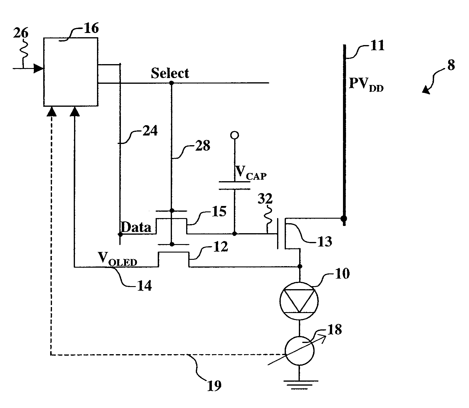
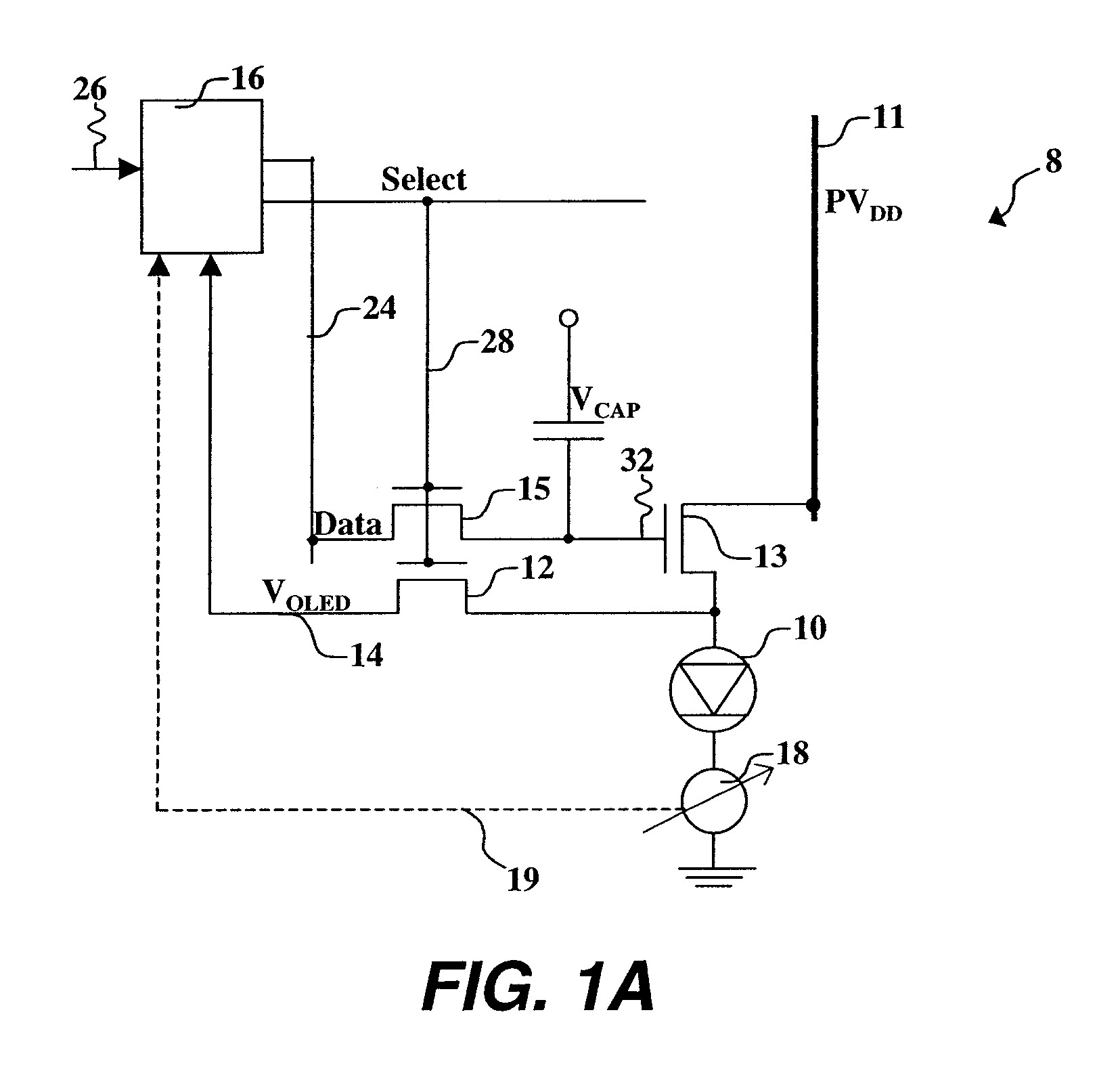
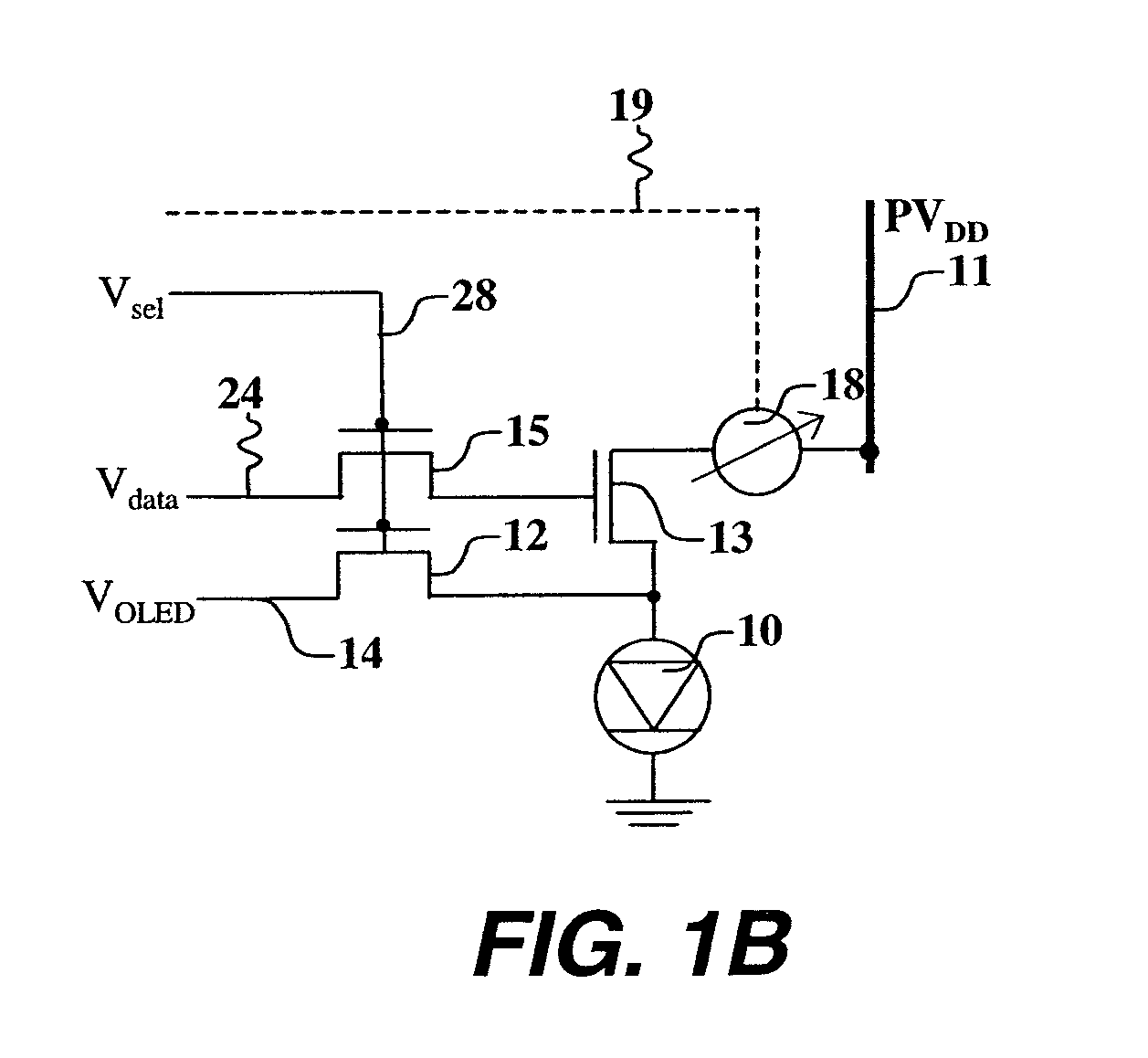
[0027]Turning now to FIG. 1A, there is shown a schematic diagram of one embodiment of a compensated drive circuit 8 adjusting for changes in the threshold voltage of a drive transistor and aging of an OLED device according to the present invention. Drive circuit 8 includes OLED device 10, drive transistor 13, a data line 24 that carries analog data (e.g. voltage) representative of the brightness level desired from OLED device 10, switch transistor 15, and a select line 28. An OLED display can comprise an array of drive circuits 8. Drive transistor 13 is connected to power supply 11 (PVDD) and to OLED device 10. Drive transistor 13 is an amorphous silicon transistor or other transistor whose properties change with time and / or use. When select line 28 is activated, switch transistor 15 is activated and a voltage from data line 24 is applied to gate electrode 32 of drive transistor 13 so that current proportional to the applied data line voltage will flow through the drain and source e...


PUM


Abstract

Compensated drive circuit adjusting for changes in the threshold voltage of a drive transistor and for aging of an OLED device, comprising: a data line carrying analog data representative of the brightness level, and a select line; the drive transistor connected to a power supply and to the OLED device such that when the select line is activated and a voltage from the data line is applied to the gate electrode of such transistor and current proportional to the applied voltage will flow through the drain and source electrodes through the OLED device; circuitry for measuring first and second parameters associated with the drive circuitry and responsive to the measured first and second parameters for computing offset voltages to adjust for changes in the threshold voltage of the drive transistors and for aging of the OLED device.

Description

FIELD OF THE INVENTION[0001]The present invention relates to solid-state OLED flat-panel displays and more particularly to such displays, which compensate for the aging of the organic light emitting display components.BACKGROUND OF THE INVENTION[0002]Solid-state organic light emitting diode (OLED) displays are of great interest as a superior flat-panel display technology. These displays utilize current passing through thin films of organic material to generate light. The color of light emitted and the efficiency of the energy conversion from current to light are determined by the composition of the organic thin-film material. Different organic materials emit different colors of light. However, as the display is used, the organic materials in the display age and become less efficient at emitting light. This reduces the lifetime of the display. The differing organic materials can age at different rates, causing differential color aging and a display whose white point varies as the dis...

Claims


Application Information

Patent Timeline
Patent Type & Authority Patents(United States)
IPC IPC(8): G09G3/32
CPCG09G3/3233G09G3/3241G09G2300/0814G09G2300/0819G09G2320/0285G09G2320/029G09G2320/0295G09G2320/041G09G2320/043G09G2320/045
Inventor LEON, FELIPE A.PARRETT, GARYWHITE, CHRISTOPHER J.
Owner GLOBAL OLED TECH
Why Eureka
Try Eureka