Liquid crystal display device

a technology of liquid crystal display and light source module, which is applied in the direction of semiconductor devices, lighting and heating apparatus, instruments, etc., can solve the problems of high application voltage still required for devices, device operation and module drive techniques that have not reached the technical level of products, and the configuration of a light source module as an illumination device has not yet been sufficiently optimized. , to achieve the effect of simple operation response and voltage control

Active Publication Date: 2008-10-23
JAPAN DISPLAY INC +1
View PDF13 Cites 22 Cited by
  • Summary
  • Abstract
  • Description
  • Claims
  • Application Information

AI Technical Summary

Benefits of technology

[0019]When a LED light source and a liquid crystal display device using the light source according to the present invention are implemented, it becomes possible to perform simple operational response and voltage control.

Problems solved by technology

Although light emitting diode devices (LED device) are mounted on a liquid crystal display device at present, the configuration of a light source module as an illumination device has not yet been sufficiently optimized.
A light source for a large scale sized liquid crystal display television has a problem in view of low power consumption and low cost which will be required for them, and accordingly techniques for device operation and module drive have not reached the technical level of products.
However, a high application voltage is still required for devices on a single wiring substrate, and each device wiring line requires a different application voltage.

Method used


Image

  • Liquid crystal display device
  • Liquid crystal display device
  • Liquid crystal display device

Examples


first embodiment

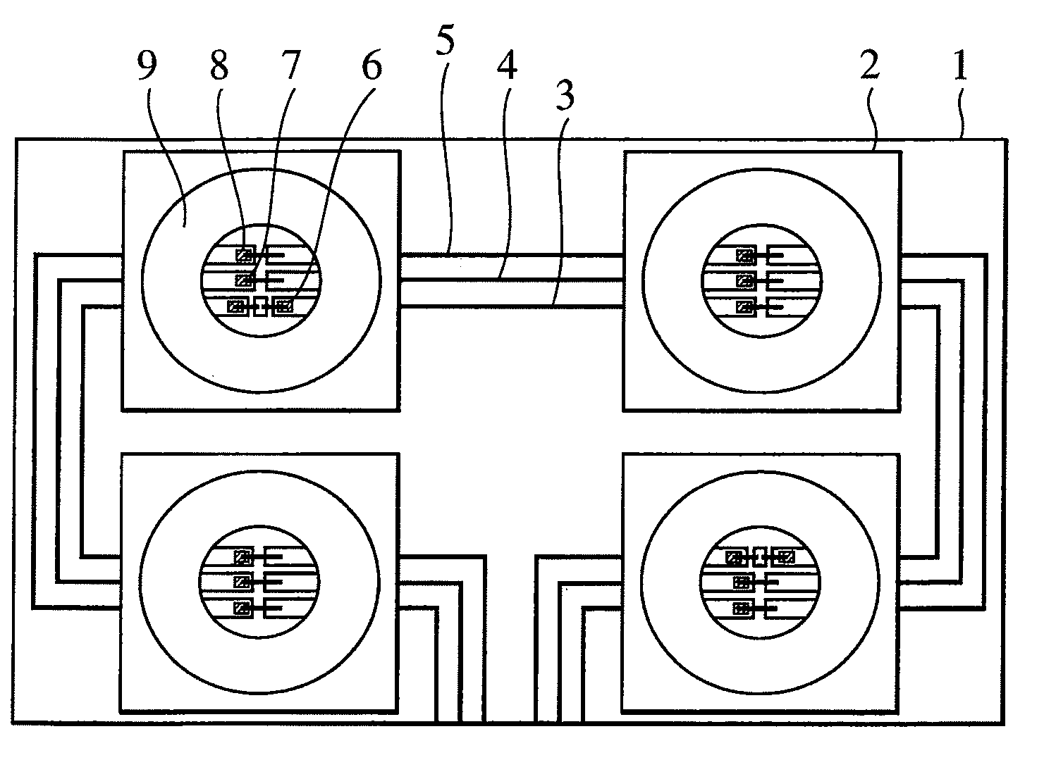
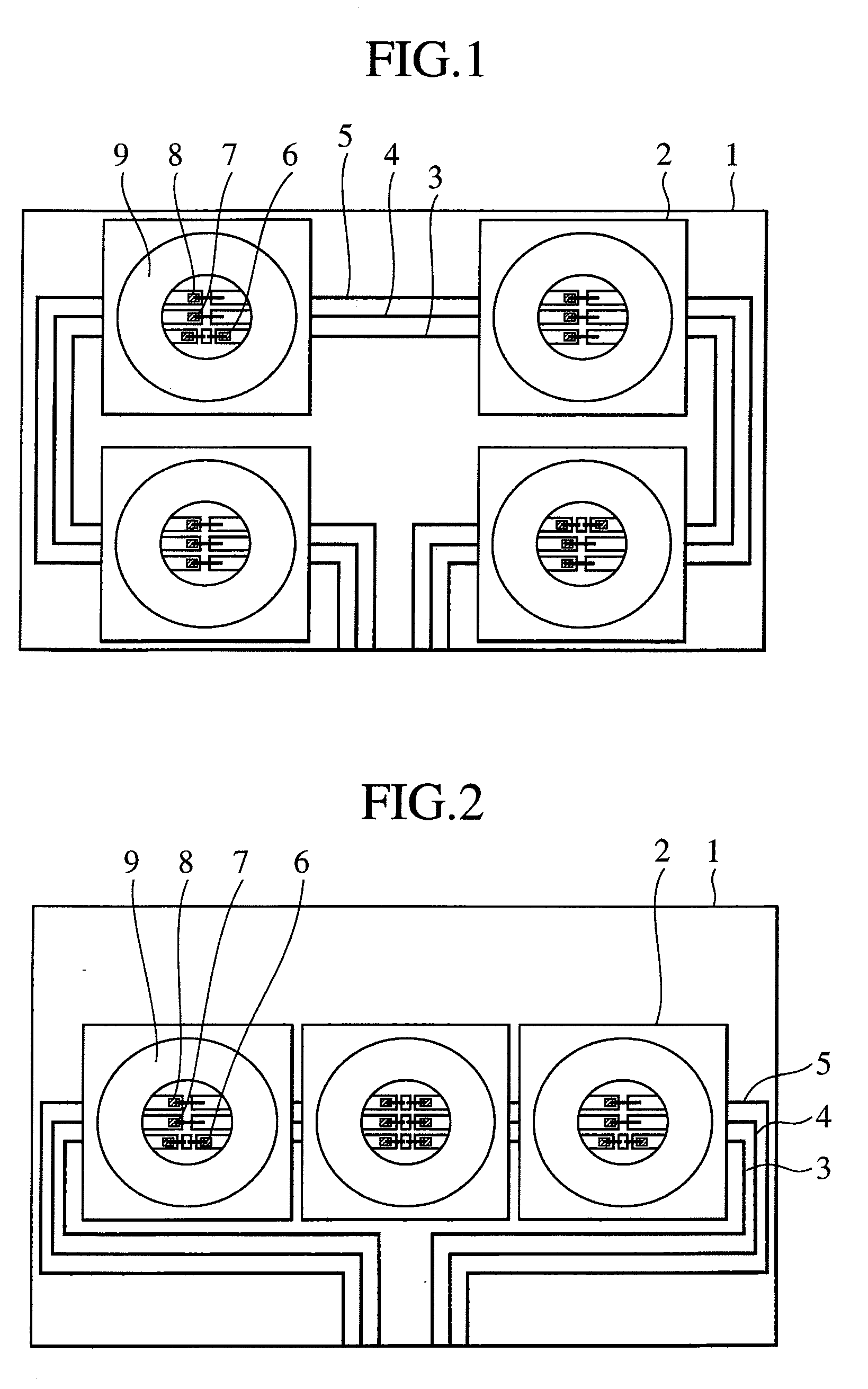
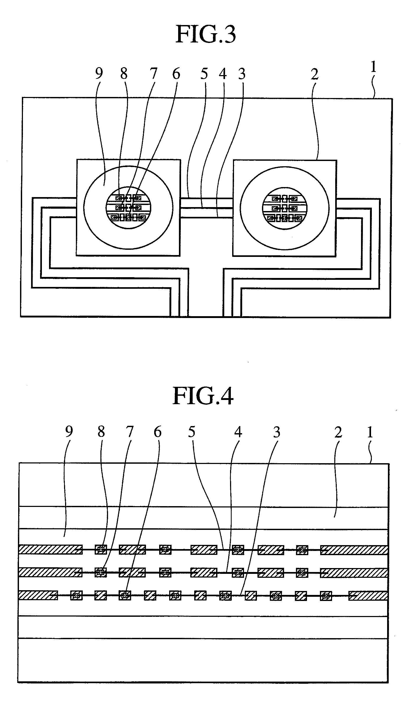
[0071]A first embodiment of the present invention will be explained below with reference to FIGS. 1 to 12.

[0072]With the first embodiment, a plurality of R-, G-, and B-LED devices are mounted on a wiring substrate, and a constant power voltage is applied to the R-, G-, and B-LED device wiring lines.

[0073]With arrangements of FIGS. 1 to 4, a reflector 2 is provided on a metal substrate with an insulating layer or a ceramic substrate 1. R-LED devices 6 (having a peak in a wavelength region from 610 nm to 640 nm), G-LED devices 7 (having a peak in a wavelength region from 510 nm to 540 nm), and B-LED devices 8 (having a peak in a wavelength region from 445 nm to 475 nm) are mounted in a R-LED device wiring line 3, a G-LED device wiring line 4, and a B-LED device wiring line 5, respectively, and sealed in a package by use of transparent resin 9. In this example, six R-LED devices, four G-LED devices, and four B-LED devices are respectively mounted in the R, G, and B wiring lines.

[0074]T...

second embodiment

[0089]A second embodiment of the present invention will be explained below with reference to FIGS. 13 to 15.

[0090]Although the present embodiment configures a wiring substrate unit like in the first embodiment, the present embodiment is characterized in that a wiring resistance is provided in advance in each of the R-, G-, and B-LED device wiring lines. In the wiring substrate unit, a difference occurs in current-voltage characteristics of R-, G-, and B-LED devices resulting in characteristic variation and, therefore, it is necessary that LED devices can be driven by a constant power voltage. In order to enable operation as a backlight of a liquid crystal display device on a required power voltage 12V, a resistance required for each of the R-, G-, and B-LED device wiring lines is monitored beforehand. It is possible to determine a difference between the monitored resistance and the actually measured resistance by comparing these values in the inspection process. During inspection, a...

third embodiment

[0095]A third embodiment of the present invention will be explained below with reference to FIGS. 16 to 28.

[0096]Similar to the second embodiment, the present embodiment configures a wiring substrate unit and is characterized in that a zener diode is provided in each of the R-, G-, and B-LED device wiring lines. The present embodiment is provided with a function to drive the LED devices on a 12V or 24V drive voltage while adjusting the resistance of resistance wiring through function trimming and performing temperature compensation of the operating voltage by use of a zener diode, simultaneously with LED device lighting inspection for each line.

[0097]First of all, an example for applying this function to the R-LED device wiring line is shown. FIG. 16 is a diagram showing a case where a zener diode is provided in the R-LED device wiring line. Four R-LED devices and a zener diode are implemented in the R-LED device wiring line. It is made possible to drive the R-LED device wiring line...


PUM

PropertyMeasurementUnit
power voltageaaaaaaaaaa
wavelength regionaaaaaaaaaa

Abstract

An illumination device using a plurality of LED light sources each of which is driven by a single power supply is provided to attain simple operational response and voltage control.
The illumination device includes a light source module, the module comprising: a substrate; a plurality of wiring lines provided on the substrate; and a plurality of LED devices implemented in the wiring lines; wherein the plurality of LED devices include a plurality of red LED devices, a plurality of green LED devices, and a plurality of blue LED devices; wherein the plurality of wiring lines include a wiring line having the plurality of red LED devices implemented in series, a wiring line having the plurality of green LED devices implemented in series, and a wiring line having the plurality of blue LED devices implemented in series; and wherein the plurality of wiring lines are connected in parallel and driven by a single power voltage.

Description

BACKGROUND OF THE INVENTION[0001]1. Field of the Invention[0002]The present invention relates to a light source module having light emitting diode devices mounted thereon and a liquid crystal display device for which they are applied as a backlight.[0003]2. Description of the Related Art[0004]Although light emitting diode devices (LED device) are mounted on a liquid crystal display device at present, the configuration of a light source module as an illumination device has not yet been sufficiently optimized. A light source for a large scale sized liquid crystal display television has a problem in view of low power consumption and low cost which will be required for them, and accordingly techniques for device operation and module drive have not reached the technical level of products.[0005]The configuration of a light source module having LED devices mounted thereon enables planar-split area control that has not been realized with the conventional CCFL technique. In planar-split area...

Claims


Application Information

Patent Timeline
Patent Type & Authority Applications(United States)
IPC IPC(8): G02F1/13357H01L27/15H01L33/50H05B44/00
CPCG09G3/3413H05B33/0821G02F2001/133612G09G2320/0233H05B33/0818G02F1/133603F21K9/50G09G2320/041G02F1/133621F21K9/60H05B45/40G02F1/133612H05B45/397Y02B20/30
Inventor TANAKA, TOSHIAKIKANEKO, HIROKIHIYAMA, IKUO
Owner JAPAN DISPLAY INC
Why Eureka
Try Eureka