
Solid-state image pick-up device

Inactive Publication Date: 2005-05-10
FUJIFILM CORP
View PDF8 Cites 9 Cited by
  • Summary
  • Abstract
  • Description
  • Claims
  • Application Information

AI Technical Summary

Benefits of technology

[0014]It is an object of the invention to provide a solid-state image pick-up device which relieves a narrow channel effect produced by a channel stopper and reduces the influence of a trapped charge and the influence of a dangling bond or a high-speed GR center.

Problems solved by technology

Consequently, a charge is insufficiently read from a photodiode (pixel) to the vertical transfer path 1 or is insufficiently transferred along the vertical transfer path 1.
In the conventional solid-state image pick-up device shown in FIG. 17, however, in the case in which a charge is stored in the vertical transfer path 1, there is a problem in that a potential difference between an interface 5 of the channel stopper 2 and the signal charge of the vertical transfer path 1 is reduced (see FIGS. 16 and 22) and a charge (an electron in the solid-state image pick-up device shown in the drawing) is apt to be trapped into the interface 5.
Consequently, the picture quality of a pick-up image is considerably deteriorated.
Therefore, there is also a problem in that the generation of a dark current from a dangling bond and the generation of a white scratch from a high-speed GR center (a heavy metal atom) are increased remarkably.

Method used


Image

  • Solid-state image pick-up device
  • Solid-state image pick-up device
  • Solid-state image pick-up device

Examples


Embodiment Construction

[0044]An embodiment of the invention will be described below with reference to the drawings.

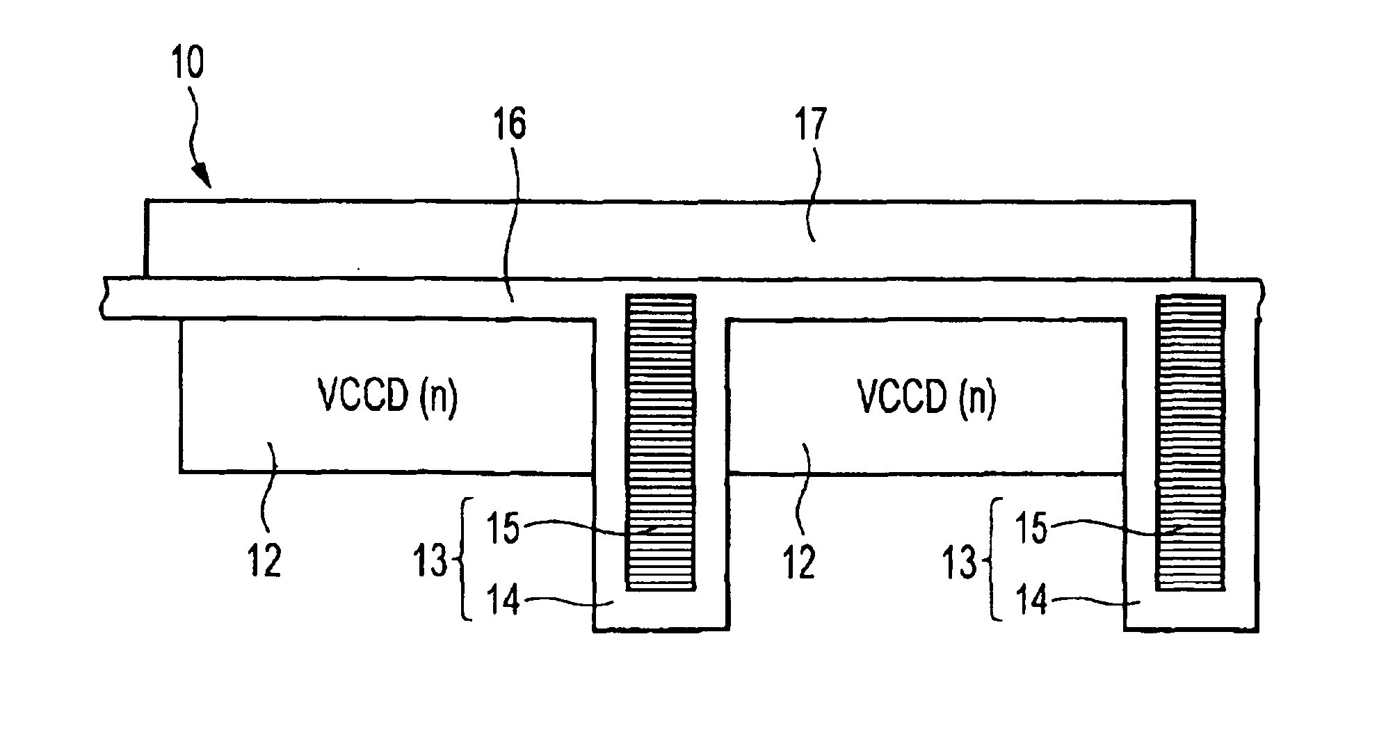
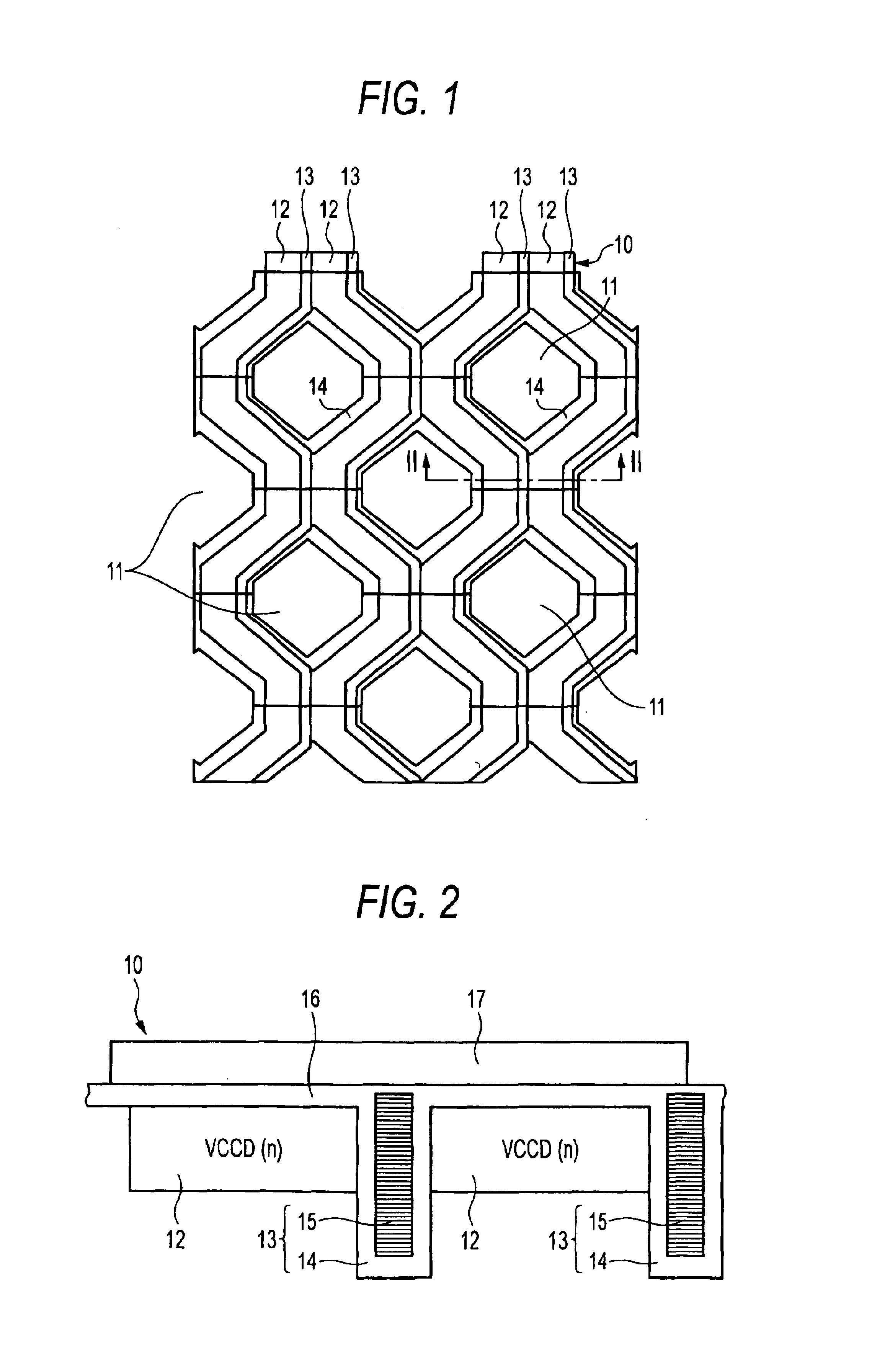
[0045]FIG. 1 is a plan view showing the main part of a solid-state image pick-up device according to a first embodiment of the invention. A solid-state image pick-up device 10 is of a so-called honeycomb type in which a pixel 11 comprising a photodiode is formed with a shift of a 1 / 2 pitch every other line in a horizontal direction. Each pixel 11 has a vertical transfer path 12 formed zigzag at both sides thereof, and a channel stopper 13 is provided on the right side of each vertical transfer path 12. Consequently, the vertical transfer path 12 is isolated from an adjacent element in portions other than a necessary region 14 for reading a charge from the pixel 11. While the embodiment is intended for the solid-state image pick-up device of the honeycomb type, the invention can also be applied to a solid-state image pick-up device of a Bayer type having a channel stopper.

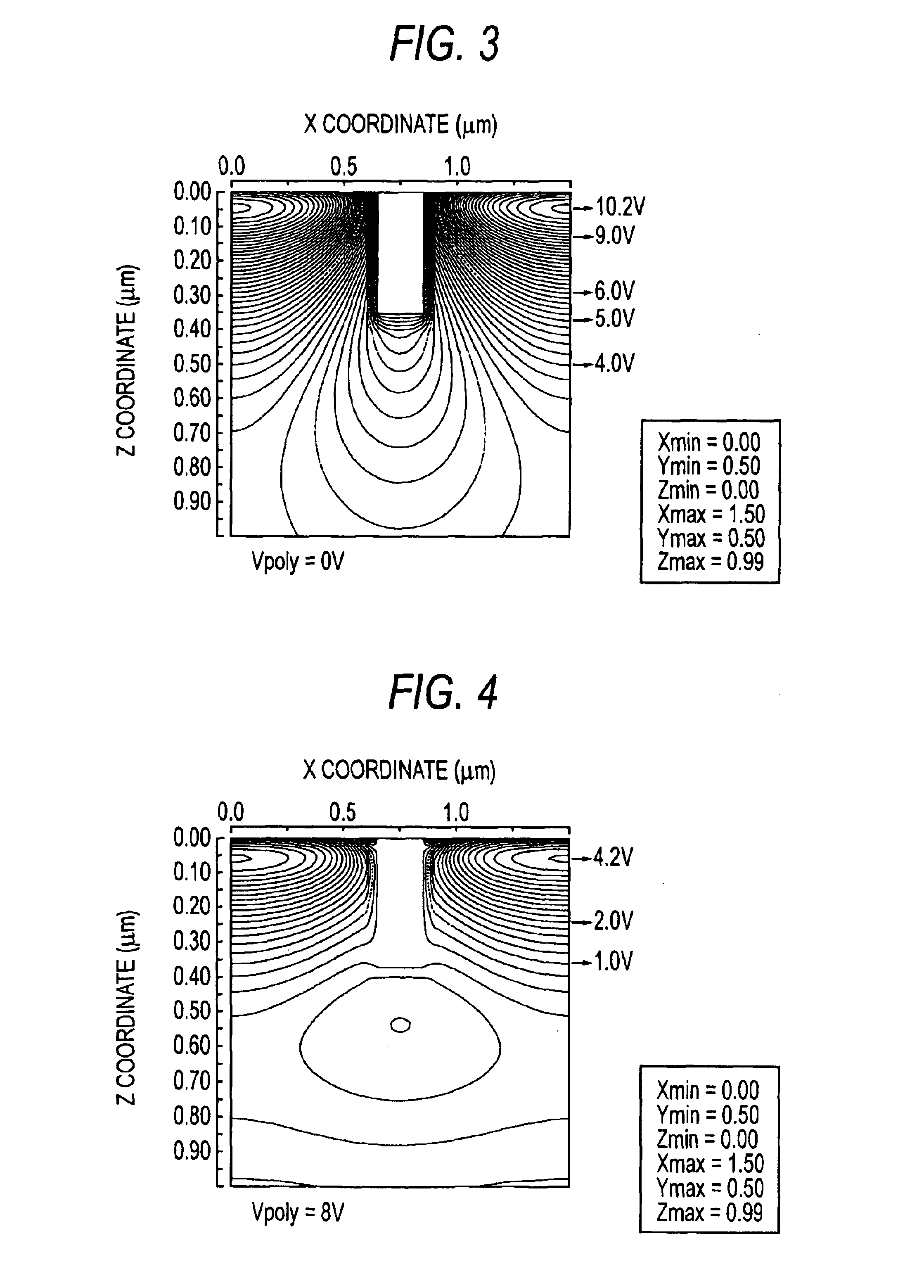
[0046]FIG. 2 is a sec...


PUM


Abstract

In a solid-state image pick-up device comprising a plurality of light receiving sensor sections, a vertical transfer path 12 formed close to each of the light receiving sensor sections, and a channel stopper 13 provided between the adjacent vertical transfer paths 12 and formed by an insulating layer having a trench structure, a conductive substance 15 to which a predetermined voltage is applied is buried in the insulating layer 14. The predetermined voltage is a negative voltage if a signal charge is an electron, and is a positive voltage if the signal charge is a hole. Alternatively, the predetermined voltage is a pulse having an opposite phase to that of a read pulse to be applied to a transfer electrode 17 of the vertical transfer path 12.

Description

BACKGROUND OF THE INVENTION[0001]1. Field of the Invention[0002]The present invention relates to a solid-state image pick-up device such as a CCD, and more particularly to a solid-state image pick-up device including a channel stopper having a trench structure for isolating adjacent elements.[0003]2. Description of the Related Art[0004]FIG. 10 is a sectional view showing the main part of a conventional solid-state image pick-up device. A vertical transfer path (VCCD) 1 in an n region is formed in the surface portion of the semiconductor substrate of the solid-state image pick-up device, and an isolation is carried out between the adjacent vertical transfer paths 1 through a channel stopper (CS) 2 constituted by a p-type impurity layer. Moreover, a transfer and read electrode 3 comprising a polycrystalline silicon is provided on the surface of the semiconductor substrate.[0005]The p-type impurity of the channel stopper 2 is diffused to the adjacent vertical transfer path 1 so that th...

Claims


Application Information

Patent Timeline
IPC IPC(8): H01L27/148H01L27/146H04N5/335H04N5/341H04N5/357H04N5/369H04N5/372
CPCH01L27/1463H01L27/14887H01L27/14831H01L27/14806
Inventor ADACHI, YUKOYAMADA, TETSUOUYA, SHINJI
Owner FUJIFILM CORP
Learn More