Exposure method and apparatus

a technology of exposure method and apparatus, applied in the field of exposure, can solve the problems of no image formation at all, and no effective polarized illumination for dense contact hole pattern found at presen

Inactive Publication Date: 2008-04-15
CANON KK
View PDF8 Cites 12 Cited by
  • Summary
  • Abstract
  • Description
  • Claims
  • Application Information

AI Technical Summary

Problems solved by technology

In particular, the recently-proposed immersion exposure problematically has a condition under which no image is formed at all due to the polarization direction of the light.
The polarization control over a contact hole pattern is also studied, because the polarized illumination suitable for the L / S pattern is not always applicable to the contact hole pattern.
Reference 3 states, however, that no effective polarized illumination is found at present for the dense contact hole pattern.

Method used


Image

  • Exposure method and apparatus
  • Exposure method and apparatus
  • Exposure method and apparatus

Examples


first embodiment

[0042]Assume that an exposure apparatus uses the exposure light having a wavelength of about 193 nm, has a projection optical system with an NA of 0.92, and sets the maximum σ to one. For a dense contact hole pattern having a hole diameter of 85 nm and a hole interval of 85 nm, an effective light source shape is set to a quadrupole illumination that has four light irradiating (or bright) parts at ±45° directions with respect to a horizontal direction (a periodic direction of the pattern) as shown in FIG. 8A. A center of each light irradiating part 81 is distant by 0.85 from the center of the effective light source shape when converted into σ. Each light irradiating part 81 has a diameter of 0.20 when converted into σ.

[0043]FIG. 9A shows a relationship between a defocus amount and a hole diameter or critical dimension (“CD”) when the mask is a binary mask. In FIG. 9A, under “10 nm bias,” the hole diameter is adjusted to 95 nm and the hole interval is adjusted to 75 nm, but the expose...

second embodiment

[0048]The polarized illumination suitable for the dense contact hole pattern has been discussed with respect to the mask type and the half pitch size. An actual contact hole mask has not only a dense contact hole pattern but also an isolated contact hole pattern. Usually, the isolated contact hole is so optically sufficiently isolated that a ratio between the hole diameter and the hole interval is 1:7 or greater. However, in a broad sense, it is isolated when the interval is such that the adjacent two holes do not affect each other and strictly speaking the ratio depends upon the effective light source shape. Therefore, a ratio between the hole diameter and the hole interval is 1:5 or greater may be entitled to the isolation. Since the range is defined as up to 1:3, this specification refers to the ratio between the hole diameter and the hole interval from 1:3 to 1:7 as an intermediate period. According to the conventional practice, a small a illumination is suitable for the isolate...

third embodiment

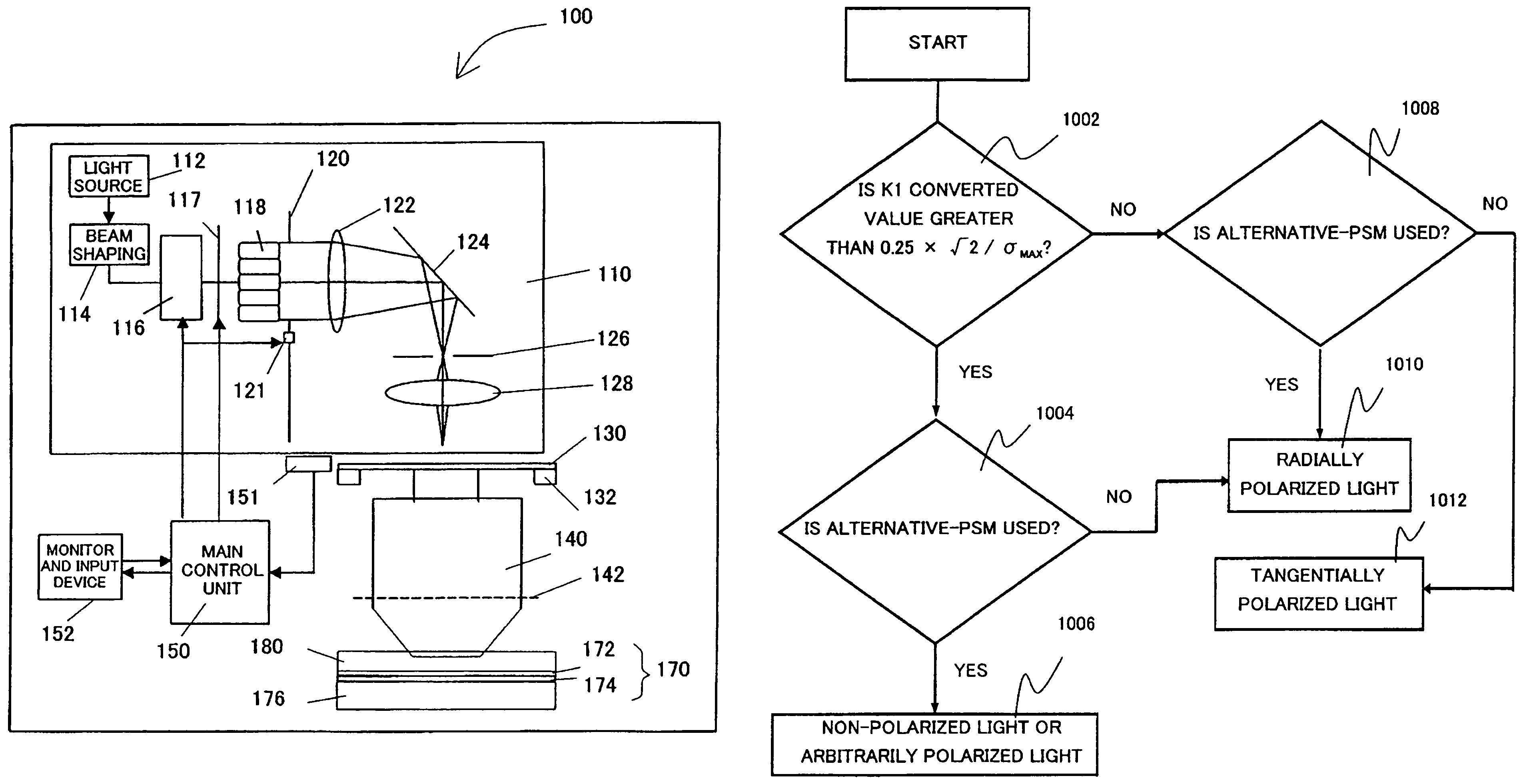
[0060]A description will now be given of an exposure apparatus 100 of one embodiment according to the present invention with reference to FIG. 1. Here, FIG. 1 is a schematic block diagram of the exposure apparatus 100. As shown in FIG. 1, the exposure apparatus includes an illumination unit 110, a mask 130, a mask stage 132, a projection optical system 140, a main control unit 150, a monitor and input device 150, a wafer 170, a wafer stage 176, and a liquid 180 as a medium. Thus, the exposure apparatus 100 is an immersion exposure apparatus that immerses a space between the final surface of the projection optical system 140 and the wafer 170 in the liquid 180, and exposes the mask patterns onto the wafer 170 via the liquid 180. Although the exposure apparatus 100 of the instant embodiment is a step-and-scan manner projection exposure apparatus (or a scanner), the present invention is applicable to a step-and-repeat manner and other exposure methods.

[0061]The illumination apparatus 1...


PUM

PropertyMeasurementUnit
transmittanceaaaaaaaaaa
wavelengthaaaaaaaaaa
hole diameteraaaaaaaaaa

Abstract

An exposure method for exposing an image of a mask pattern onto a plate via a projection optical system. The method includes a step of illuminating one of a binary mask and an attenuated phase shifting mask, which has a contact hole pattern and an auxiliary pattern, by utilizing light from a light source and an illumination optical system so that the contact hole pattern can be resolved, but a resolution of the auxiliary pattern is restrained. The illuminating step uses an off-axis illumination that is polarized in a tangential direction when a value that is calculated by normalizing half the length of an interval between centers of the auxiliary pattern and the contact hole pattern that are adjacent to each other by λ / NA is 0.25×√{square root over (2)} or smaller, where λ is a wavelength of the light, and NA is a numerical aperture of the projection optical system at an image side.

Description

BACKGROUND OF THE INVENTION[0001]The present invention relates generally to exposure, and, more particularly, to an exposure method and apparatus, and a method of manufacturing various devices including semiconductor chips such as ICs and LSIs, display devices such as liquid crystal panels, sensing devices such as magnetic heads, and image pick-up devices such as CCDs, as well as a mask used for micromechanics. Here, the term micromechanics refers to technology for applying the semiconductor IC fabricating technique for fine structure fabrications, thereby creating an enhanced mechanical system that may operate at a level of a micron. The inventive exposure method and apparatus are suitable, for example, for so-called immersion exposure that immerses, in a liquid, a space between a surface of a plate to be exposed and a final surface of a projection optical system, and to expose the plate via the projection optical system and the liquid.[0002]A conventional projection exposure appar...

Claims


Application Information

Patent Timeline
Patent Type & Authority Patents(United States)
IPC IPC(8): G03B27/42G03F7/20H01L21/027
CPCG03F7/70125G03F7/70566G03F1/144G03F1/00G03F1/32G03F1/36G03F1/38
Inventor YAMAZOE, KENJI
Owner CANON KK
Why Eureka
Try Eureka