Method for fabricating semiconductor device capable of preventing scratch

a technology of semiconductor devices and manufacturing methods, applied in the direction of semiconductor devices, basic electric elements, electrical appliances, etc., can solve the problems of generating various defects, and reducing the yield of products, so as to reduce the height difference, and improve the yield

Inactive Publication Date: 2008-04-22
SK HYNIX INC
View PDF8 Cites 2 Cited by
  • Summary
  • Abstract
  • Description
  • Claims
  • Application Information

AI Technical Summary

Benefits of technology

[0015]It is, therefore, an object of the present invention to provide a method for fabricating a semiconductor device capable of removing metal particles generated during depositing a plate electrode that cause scratches during a chemical mechanical polishing process with respect to a subsequent inter-layer insulation layer for reducing a height difference between a cell region and a peripheral region.
[0016]In accordance with one aspect of the present invention, there is provided a method for fabricating a semiconductor device, including the steps of: forming a substrate divided into a peripheral region and a cell region where a capacitor including a metal plate electrode on which particles with a pointed shape are generated is formed; forming an inter-layer insulation layer with a poor step coverage on the metal plate electrode, the particles with the pointed shape and a surface of the substrate in the peripheral region; etching a portion of the inter-layer insulation layer, thereby exposing predetermined portions of lateral sides of the particles with the pointed shape; selectively removing the exposed portions of the particles with the pointed shape to separate top portions of the particles with the pointed shape from the inter-layer insulation layer; and planarizing the inter-layer insulation layer through a chemical mechanical polishing (CMP) process for reducing a height difference between the cell region and the peripheral region.

Problems solved by technology

However, the conventional method generates various defects when said anther TiN layer that is the top layer of the plate electrode 17 is deposited through performing the CVD method.
These scratches provide a high possibility of forming a bridge during forming a subsequent metal interconnection line, thereby degrading yields of products.
As a result, the conventional method causes a lot of scratches since several large particles generated before the CMP process performed to the target inter-layer insulation layer are not polished and continuously remain.
Thus, the conventional method brings out a problem of degrading the yields of semiconductor devices.

Method used


Image

  • Method for fabricating semiconductor device capable of preventing scratch
  • Method for fabricating semiconductor device capable of preventing scratch
  • Method for fabricating semiconductor device capable of preventing scratch

Examples


Embodiment Construction

[0020]Hereinafter, detailed descriptions on preferred embodiments of the present invention will be provided with reference to the accompanying drawings.

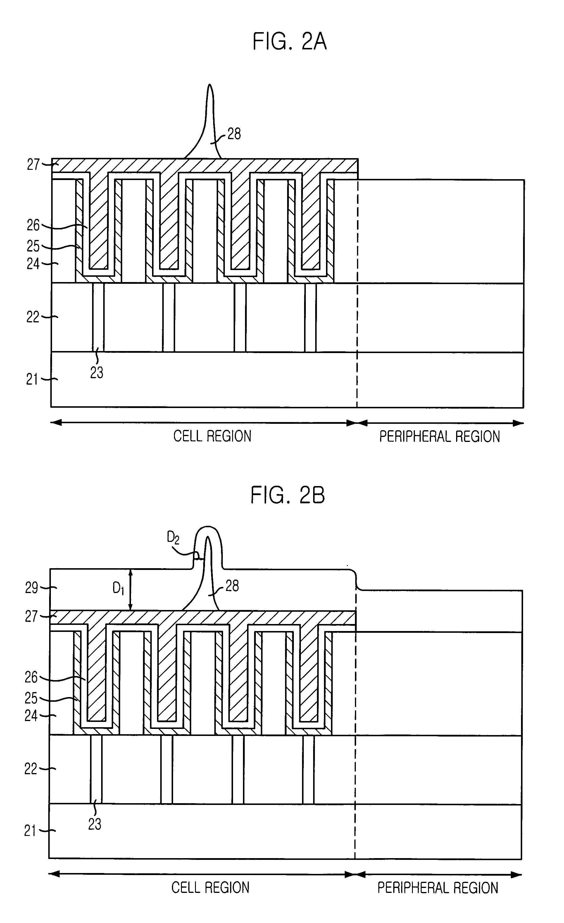
[0021]FIGS. 2A to 2E are cross-sectional views illustrating a method for fabricating a semiconductor device in accordance with the preferred embodiment of the present invention.

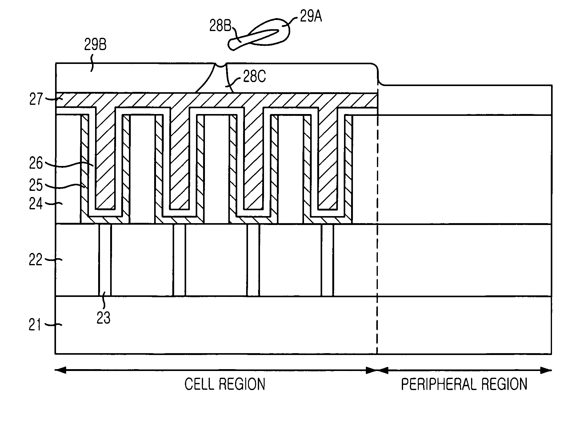
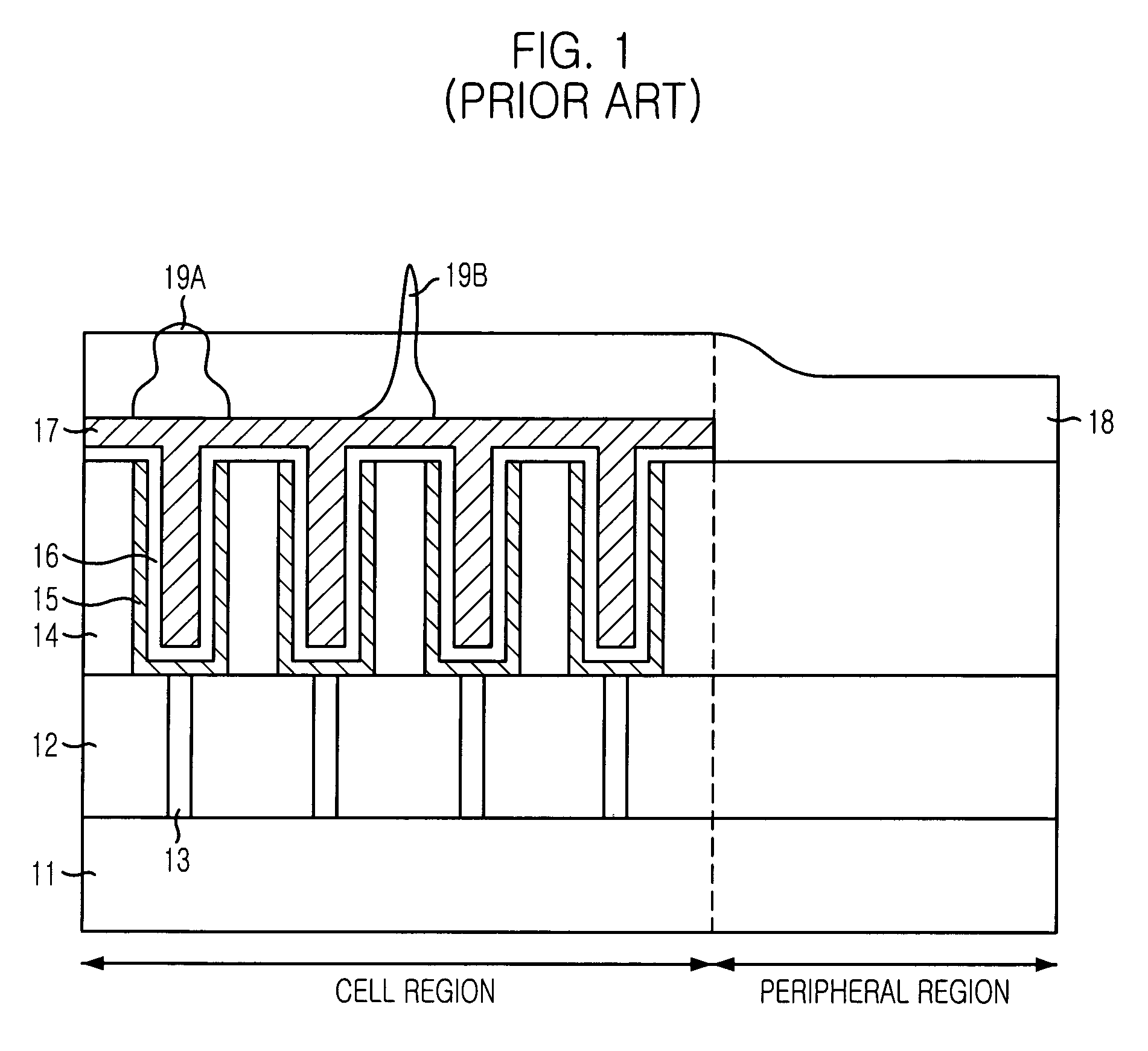
[0022]Referring to FIG. 2A, a first inter-layer insulation layer 22 is formed on a substrate 21 divided into a cell region and a peripheral region. A plurality of storage node contacts 23 connected to predetermined portions of the substrate 21 by passing through the first inter-layer insulation layer 22 are formed.

[0023]Subsequently, before the first inter-layer insulation layer 22 is formed, as usually known, other device elements such as a transistor and a bit line are formed. Accordingly, the first inter-layer insulation layer 22 can be a multi-layer structure, and a plurality of landing plug contacts can be formed beneath the plurality of storage node cont...


PUM

PropertyMeasurementUnit
temperatureaaaaaaaaaa
shapeaaaaaaaaaa

Abstract

Disclosed is a method for fabricating a semiconductor device capable of preventing scratches. The method includes the steps of: forming a substrate divided into a peripheral region and a cell region where a capacitor including a metal plate electrode on which particles with a pointed shape are generated is formed; forming an inter-layer insulation layer with a poor step coverage on the metal plate electrode, the particles with the pointed shape and a surface of the substrate in the peripheral region; etching a portion of the inter-layer insulation layer, thereby exposing predetermined portions of lateral sides of the particles with the pointed shape; selectively removing the exposed portions of the particles with the pointed shape to separate top portions of the particles with the pointed shape from the inter-layer insulation layer; and planarizing the inter-layer insulation layer through a chemical mechanical polishing (CMP) process.

Description

FIELD OF THE INVENTION[0001]The present invention relates to a method for fabricating a semiconductor device; and more particularly, to a method for fabricating a semiconductor device capable of preventing scratches generated during a chemical mechanical polishing (CMP) process.DESCRIPTION OF RELATED ARTS[0002]As a scale of integration of a semiconductor device has increased, the need of forming a plurality of interconnection lines has been increased. To form the plurality of interconnection lines, a role of an inter-layer insulation layer is very important. The inter-layer insulation layer serves the role in insulating a bottom interconnection line and a top interconnection line from each other. A planarization of the inter-layer insulation layer greatly affects a planarization and a photolithography margin of a top layer to be subsequently formed.[0003]Normally, a chemical mechanical polishing (CMP) process is mainly used for planarizing the inter-layer insulation layer. The metho...

Claims


Application Information

Patent Timeline
Patent Type & Authority Patents(United States)
IPC IPC(8): H01L21/302H01L21/461
CPCH01L21/31053H01L21/3212H01L27/10852H01L27/10894Y10S438/906H10B12/033H10B12/09H01L21/3205H01L27/04H01L21/304
Inventor YOON, YANG-HAN
Owner SK HYNIX INC
Why Eureka
Try Eureka