Semiconductor Devices and Microphones

A technology for semiconductors and microphones, which is applied in the directions of semiconductor devices, semiconductor electrostatic transducers, semiconductor/solid-state device components, etc., can solve the problems of complicated packaging structure, increased manufacturing cost of microphones, and inability to reduce the wall thickness of side walls.

Inactive Publication Date: 2011-12-14
ORMON CORP
View PDF10 Cites 15 Cited by
  • Summary
  • Abstract
  • Description
  • Claims
  • Application Information

AI Technical Summary

Problems solved by technology

However, in the structure of Patent Document 4, it is necessary to form a structure such as a through hole and a coil spring in the side wall of the cover, which complicates the packaging structure and increases the production cost of the microphone.
In addition, since the thickness of the side wall cannot be reduced, there is a problem that the mounting area of ​​the package increases.

Method used


Image

  • Semiconductor Devices and Microphones
  • Semiconductor Devices and Microphones
  • Semiconductor Devices and Microphones

Examples


no. 1 approach

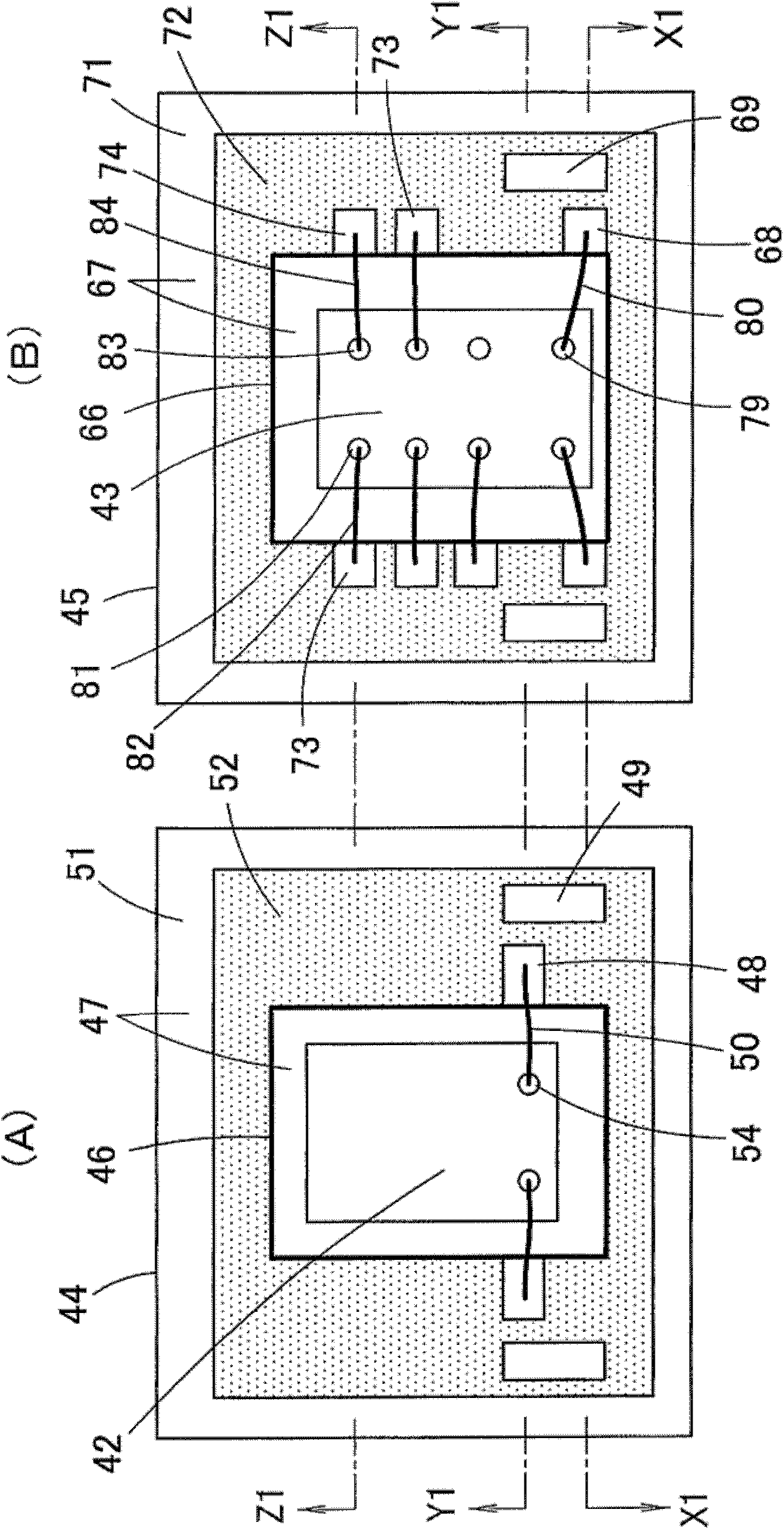
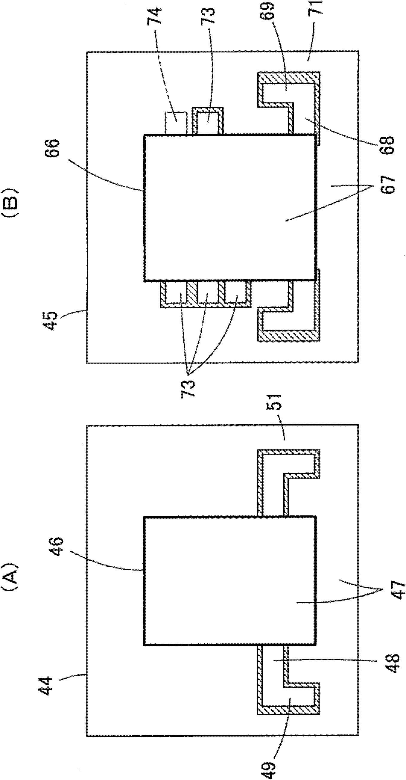
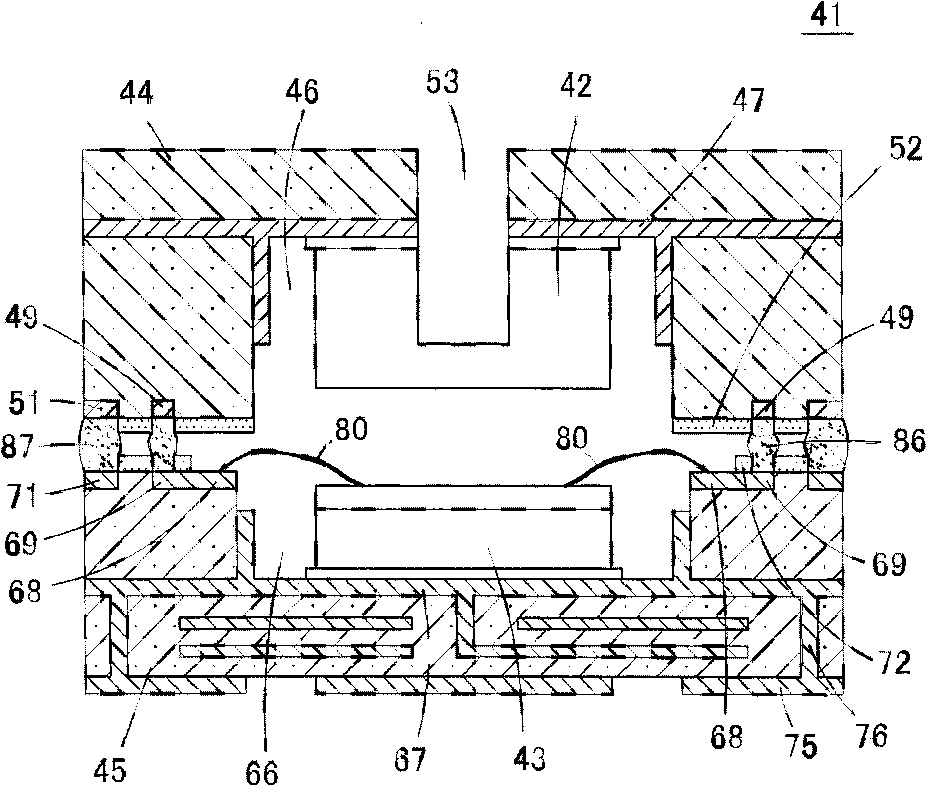
[0085] Reference Figure 1 ~ Figure 4 The top-mouth microphone 41 according to Embodiment 1 of the present invention will be described. The microphone 41 is a MEMS microphone manufactured using MEMS technology, and is a microphone that houses a microphone chip 42 (sensor) and circuit elements 43 in a package composed of a cover 44 (first component) and a substrate 45 (second component). In addition, in the microphone 41 of the first embodiment, a sound hole 53 is opened in the cover 44 to be a top mouth type. figure 1 (A) is a bottom view of the cover 44 with the microphone chip 42 installed, figure 1 (B) is a plan view of the substrate 45 on which the circuit element 43 is mounted. figure 2 (A) is a bottom view of the cover 44 with the solder mask removed, figure 2 (B) is a plan view of the substrate 45 with the solder resist film removed. In addition, image 3 Is equivalent to figure 1 A cross-sectional view of the microphone 41 along the line X1-X1. Figure 4 Is equivale...

no. 2 approach

[0106] Then, pass Figure 9~Figure 11 The ceiling-hole microphone 91 of the second embodiment will be described. Picture 9 (A) is a bottom view of the cover 44 with the microphone chip 42 installed, Picture 9 (B) is a plan view of the substrate 45 on which the circuit element 43 is mounted. In addition, Picture 10 Is equivalent to Picture 9 A cross-sectional view of the microphone 91 at the line X2-X2. Picture 11 Is equivalent to Picture 9 A cross-sectional view of the microphone 91 at the Y2-Y2 line. In addition, the present embodiment has substantially the same structure as the first embodiment, so in the drawings, the same reference numerals are assigned to the parts with the same structure as in the first embodiment, and the description thereof is omitted (the same applies after the third embodiment).

[0107] In the microphone 91, a sound hole 53 is opened in the recess 46 of the cover 44 at a position that does not overlap the microphone chip 42. Therefore, in the microph...

no. 3 approach

[0109] Picture 12 (A) and Picture 12 (B) is a diagram illustrating a bottom hole type microphone according to Embodiment 3 of the present invention. Picture 12 (A) is a bottom view of the cover 44 with the microphone chip 42 installed, Picture 12 (B) is a plan view of the substrate 45 on which the circuit element 43 is mounted. In addition, equivalent to Picture 12 The cross-section of the microphone of Embodiment 3 at the X3-X3 line and Picture 10 Same, equivalent to Picture 12 The cross-section of the microphone of Embodiment 3 at the Y3-Y3 line and Picture 11 the same.

[0110] In the microphone of Embodiment 3, in the recess 66 of the substrate 45, a sound hole 53 is opened at a position that does not overlap the circuit element 43, and is a bottom hole type. Therefore, in this microphone, the internal space of the package is also the front chamber, the opening of the Si substrate is the back chamber, and the microphone chip 42 vibrates the diaphragm by the sound arriv...


PUM


Abstract

This invention provides a semiconductor device (in particular, microphone) having a small mounting area. A package is formed by overlapping a cover (44) and a substrate (45) one over the other. A microphone chip (42) is mounted on a top surface of a recess (46) of the cover (44), and a circuit element 43 is mounted on an upper surface of a recess (66) of the substrate (45), where the microphone chip (42) is positioned perpendicularly, on the upper side of the circuit element (43). The microphone chip (42) is connected to a bonding pad arranged on the lower surface of the cover (44) by a bonding wire, the circuit element (43) is connected to a bonding pad (68) arranged on the upper surface of the substrate (45) by a bonding wire (80), and a cover side joining portion (49) conducted to the bonding pad on the lower surface of the cover (44) and a substrate side joining portion (69) conducted t to the bonding pad (68) on the upper surface of the substrate (45) are joined by a conductive material (86).

Description

Technical field [0001] The present invention relates to a semiconductor device and a microphone, and more specifically, to a semiconductor device in which a semiconductor element is housed in a package. In addition, it relates to a microphone containing a microphone chip (sound sensor) in a package. Background technique [0002] Electronic devices, especially portable devices, are required to be downsized. Therefore, high-density mounting of parts on small circuit boards is required. Furthermore, in order to enable high-density mounting of parts, it is required to reduce the occupied area (hereinafter referred to as the mounting area) during the part mounting. However, in the case of a MEMS microphone, the microphone chip and the circuit element are mounted in the package, but in the conventional microphone, the microphone chip and the circuit element are arranged side by side on the same surface of the package substrate or cover. Therefore, reducing the installation area of ​​...

Claims


Application Information

Patent Timeline
Patent Type & Authority Applications(China)
IPC IPC(8): B81B7/02B81C1/00H04R1/00H04R19/00
CPCH01L2924/3025H01L2224/32225H01L2224/48227B81C1/00H01L2224/73265H01L2224/48465H04R19/005B81C1/0023B81B7/00H01L2224/48091B81B2201/0257B81B7/0064H04R19/04H01L2924/1461H01L2924/15153H01L2924/00014H01L2924/00H01L25/16
Inventor 鞍谷直人前川智史
Owner ORMON CORP
Why Eureka
Try Eureka