Transverse electric field liquid crystal display device picture element, and its substrate and picture element process

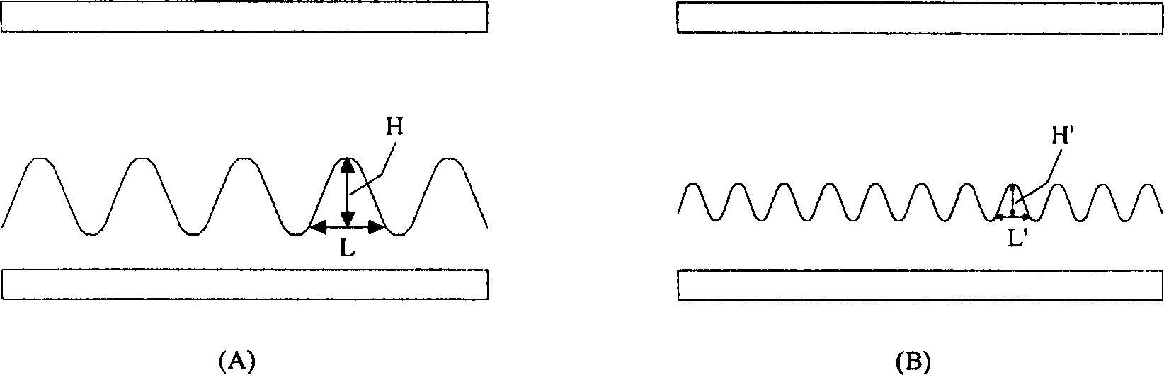
A technology of liquid crystal display and transverse electric field, which is applied in the direction of instruments, transistors, optics, etc. It can solve the problems of reducing contrast, large height difference on rough surface, narrow viewing angle, etc., and achieves reducing gap changes, good anti-glare effect, and large scatter The effect of the angle

Inactive Publication Date: 2005-07-20
WISTRON OPTRONICS CORP
View PDF0 Cites 14 Cited by
  • Summary
  • Abstract
  • Description
  • Claims
  • Application Information

AI Technical Summary

Problems solved by technology

[0002] In the prior art, a liquid crystal display (LCD) uses a TN mode and an STN mode. However, the LCDs of the TN mode and the STN mode have the disadvantage of a narrow viewing angle. Therefore, a transverse electric field (in -plane switching; IPS) LCD, in addition to having a wide viewing angle, the IPS mode LCD also has the advantages of no compensation film and fast response time, and its process has one less photomask than the TN mode LCD. However, the IPS mode LCD The pixel electrode (pixel electrode) and the common electrode (counter electrode) are made of opaque metal and have a smooth surface, so the reflection is specular reflection, thus reducing the contrast. Although, the pixel electrode and the common electrode can be A rough surface made of organic material, such as resin, is formed below to improve this shortcoming. However, increasing the organic material requires more photomasks, which increases the complexity and cost of the process, and the organic material The heat resistance is not good, about 250 degrees. In addition, because the height difference of the rough surface is too large, between 0.5um and 1.5um, the gap of the liquid crystal display changes too much, which reduces the efficiency of reflected light. The ideal 100% drops to between 60% and 85%

Method used


Image

  • Transverse electric field liquid crystal display device picture element, and its substrate and picture element process
  • Transverse electric field liquid crystal display device picture element, and its substrate and picture element process
  • Transverse electric field liquid crystal display device picture element, and its substrate and picture element process

Examples


Embodiment Construction

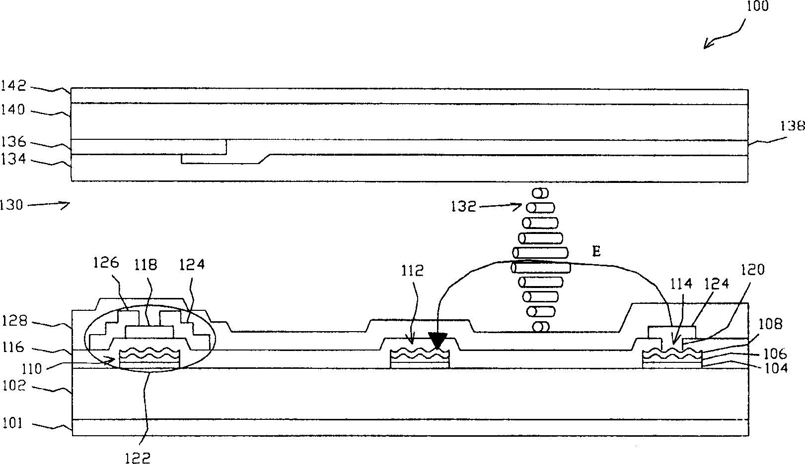
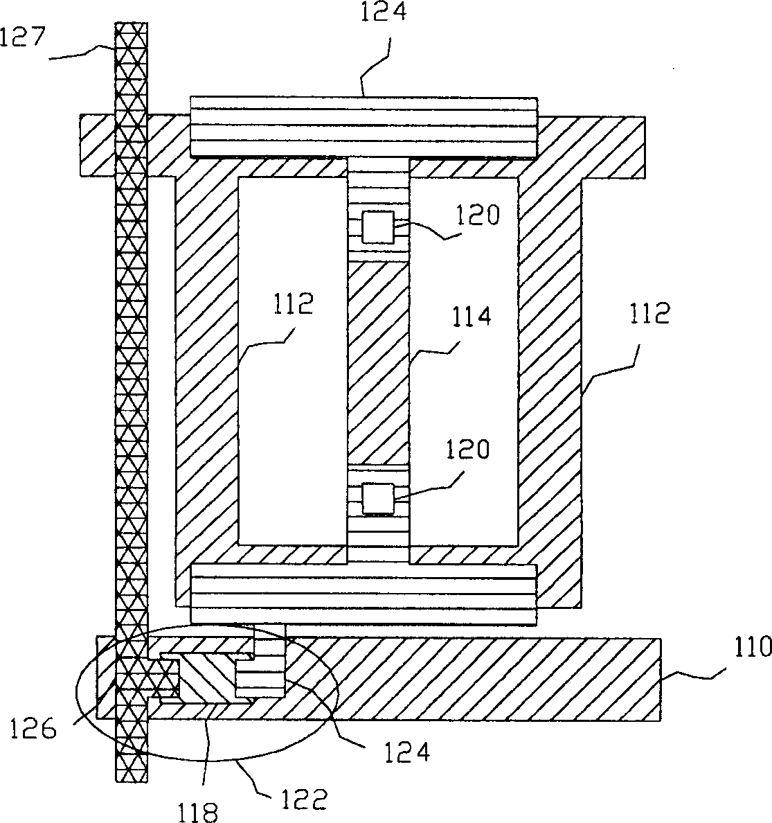
[0040] figure 1 It is an embodiment of the horizontal electric field liquid crystal display pixel structure 100 of the present invention, which is a transflective LCD, including a first structure with a nanoscale rough surface on the substrate 102, the first structure includes a first part and a second Two parts, wherein the first part is the gate electrode 110, and the second part is the reflectors 112 and 114, a protective layer 116 covers the first structure, and a second structure is the protective layer 116 above the gate electrode 110 Above, the second structure includes a drain electrode 124, a source electrode 126 and a channel region formed by an amorphous silicon semiconductor film 118 between the drain electrode 124 and the source electrode 126, the gate electrode 110 and the second structure form a switching element-thin film transistor 122, and the drain electrode 124 is connected to the reflector 114 through the through hole (contact hole) 120 on the protective l...


PUM


Abstract

This invention discloses the pels and motherboard of a kind of transverse electric field liquid crystal display and the pels technics. Its reflecting board has nanometer rank rough surface to diffuse lamp-house and increase the contrast. Besides, because the rough surface is nanometer rank, it will have bigger disheveled angle and planar effect in the aspect of disheveled effect. That is the reflectivity won't acutely change with the visual angle, and has good resist glaring effect. Furthermore the rough surface are formed by using the crystal and the characteristic of the material itself, and don't need additive light sheltering modulus.

Description

technical field [0001] The invention relates to a transverse electric field liquid crystal display, in particular to a pixel and a process of a transverse electric field liquid crystal display with a nanoscale rough surface reflector. Background technique [0002] In the prior art, a liquid crystal display (LCD) uses a TN mode and an STN mode. However, the LCDs of the TN mode and the STN mode have the disadvantage of a narrow viewing angle. Therefore, a transverse electric field (in -plane switching; IPS) LCD, in addition to having a wide viewing angle, the IPS mode LCD also has the advantages of no compensation film and fast response time, and its process has one less photomask than the TN mode LCD. However, the IPS mode LCD The pixel electrode (pixel electrode) and the common electrode (counter electrode) are made of opaque metal and have a smooth surface, so the reflection is specular reflection, thus reducing the contrast. Although, the pixel electrode and the common ele...

Claims


Application Information

Patent Timeline
Patent Type & Authority Applications(China)
IPC IPC(8): G02B5/23G02F1/1343G02F1/136H01L29/786
Inventor 刘鸿达
Owner WISTRON OPTRONICS CORP
Why Eureka
Try Eureka