Inorganic electroluminescent display device and method of manufacturing the same

a technology of electroluminescent display device and inorganic electroluminescent, which is applied in the direction of discharge tube luminescnet screen, discharge tube/lamp details, electric discharge lamps, etc., can solve the problems of reducing the lifespan of main components, affecting the efficiency of light coupling, and adding driver ic complications, etc., to achieve the effect of improving light coupling efficiency and manufacturing method

Active Publication Date: 2008-04-22
SAMSUNG DISPLAY CO LTD
View PDF9 Cites 4 Cited by
  • Summary
  • Abstract
  • Description
  • Claims
  • Application Information

AI Technical Summary

Benefits of technology

[0022]The present invention provides an inorganic electroluminescent display device having improved light coupling efficiency and a method of manufacturing the same.

Problems solved by technology

Therefore, the optical loss and luminance reduction in a corresponding display device is significant.
While this may improve luminance, it adds complications for a driver IC.
Also, increasing the supply voltage decreases the lifespan of main components and increases power consumption.
However, according to this technique, optical loss may still be caused by reflection in the prism lens.
Additionally, since most of the light that is not externally outputted due to total reflection is generated in the interface between the luminescent layer and the insulation layer, improvement of the light coupling efficiency may be slight.
However, though this technique may be effective when applied to an organic electroluminescent display device in which most of the total reflection is generated at an interface between the substrate and the electrode, it is not effective when applied to an inorganic electroluminescent display device in which most of the total reflection is generated at an interface between the luminescent layer and the insulation layer.

Method used


Image

  • Inorganic electroluminescent display device and method of manufacturing the same
  • Inorganic electroluminescent display device and method of manufacturing the same
  • Inorganic electroluminescent display device and method of manufacturing the same

Examples


first embodiment

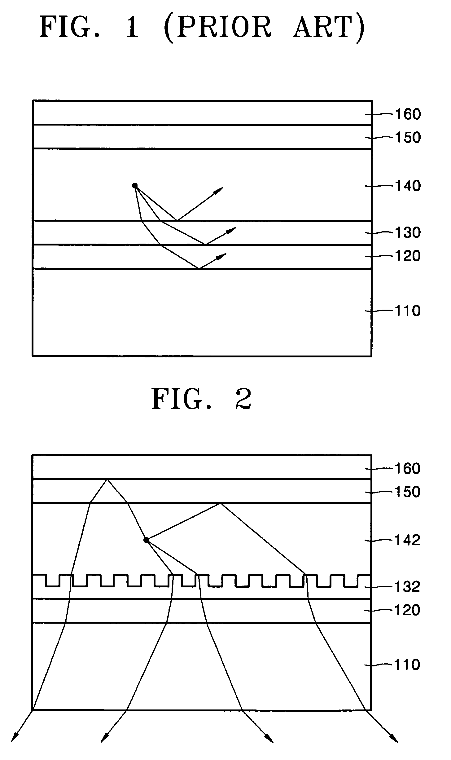
[0040]FIG. 2 is a cross-sectional view showing an inorganic electroluminescent display device according to the present invention.

[0041]As FIG. 2 shows, an inorganic electroluminescent display device according to a first embodiment of the present invention may include a substrate 110, a first electrode 120, a first insulation layer 132, a luminescent layer 142, a second insulation layer 150, and a second electrode 160, which has a different polarity from the first electrode 120. Further, a diffraction grid may be provided at an interface between the first insulation layer 132 and the luminescent layer 142. Although not shown in the drawing, a shielding member may be further provided on the second electrode 160 to shield the underlying layers. Hereinafter, for the sake of convenience, embodiments of the present invention will be described without referring to the shielding member.

[0042]The substrate 110 may be made of a transparent glass material comprising, for example, SiO2. Althoug...

second embodiment

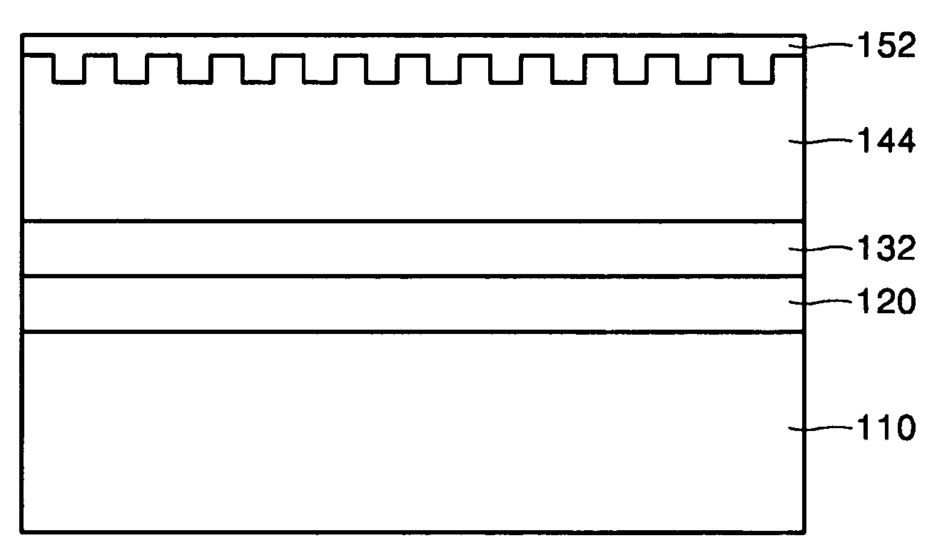
[0067]FIG. 4 is a cross-sectional view illustrating an inorganic electroluminescent display device according to the present invention, utilizing a basic principle of Equation 3.

[0068]The inorganic electroluminescent display device according to a second embodiment of the present invention includes a first electrode 120, a first insulation layer 130, a luminescent layer 144, a second insulation layer 152, and a second electrode 160 arranged on a substrate 110. Further, a diffraction grid is provided at an interface between the luminescent layer 144 and the second insulation layer 152. In this structure, light incident from the luminescent layer 144 to the second insulation layer 152 at an angle exceeding a critical angle experiences total reflection without the diffraction grid. Then, the reflected light would also be incident to the first insulation layer 130 at an angle exceeding a critical angle to experience total reflection again. Accordingly, this light is not externally outputt...

third embodiment

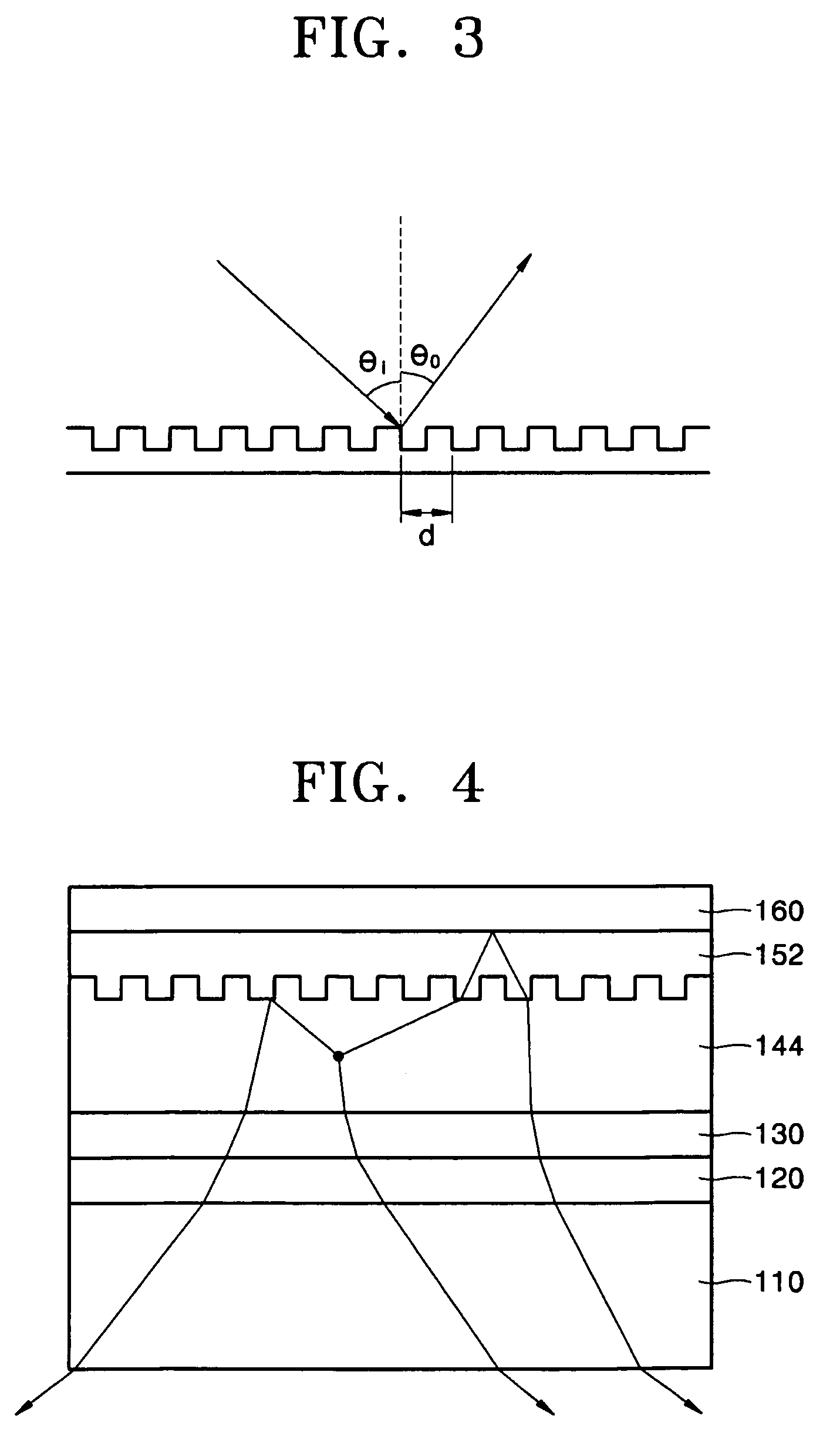
[0070]FIG. 5 is a cross-sectional view showing an inorganic electroluminescent display device according to the present invention.

[0071]As shown in FIG. 5, the inorganic electroluminescent display device according to a third embodiment of the present invention includes a first electrode 120, a first insulation layer 132, a luminescent layer 146, a second insulation layer 152, and a second electrode 160 formed on a substrate 110. Further, a first diffraction grid is provided at an interface between the luminescent layer 146 and the first insulation layer 132, and a second diffraction grid is provided at an interface between the luminescent layer 146 and the second insulation layer 152. In this structure, when light generated in the luminescent layer 146 is incident to the second insulation layer 152 at an angle exceeding a critical angle, the light is not totally reflected but diffracted by the diffraction grid formed at the interface between the luminescent layer 146 and the second i...


PUM

PropertyMeasurementUnit
thickaaaaaaaaaa
temperatureaaaaaaaaaa
size ratioaaaaaaaaaa

Abstract

An inorganic electroluminescent display device including a substrate, a first electrode formed on the substrate, a first insulation layer formed on the first electrode, a luminescent layer formed on the first insulation layer, a second insulation layer formed on the luminescent layer, and a second electrode formed on the second insulation layer. A diffraction grid is provided at at least one of a first interface between the first insulation layer and the luminescent layer and a second interface between the second insulation layer and the luminescent layer.

Description

CROSS REFERENCE TO RELATED APPLICATION[0001]This application claims priority to and the benefit of Korean Patent Application No. 10-2004-0061086, filed on Aug. 3, 2004, which is hereby incorporated by reference for all purposes as if fully set forth herein.BACKGROUND OF THE INVENTION[0002]1. Field of the Invention[0003]The present invention relates to an inorganic electroluminescent display device and a method of manufacturing the same, and more particularly, to an inorganic electroluminescent display device having improved light emission efficiency.[0004]2. Discussion of the Background[0005]Generally, an external light coupling efficiency ηex of an inorganic electroluminescent display device is given by:[0006]ηex=ηin·ηout,[Equation⁢⁢1][0007]where, ηin and ηout denote an internal light coupling efficiency and an output coupling efficiency, respectively. The internal light coupling efficiency ηin is determined by self-elimination within each layer, and the output coupling efficiency ...

Claims


Application Information

Patent Timeline
Patent Type & Authority Patents(United States)
IPC IPC(8): H01J1/62
CPCH05B33/10H05B33/145H05B33/22H01L51/5268H10K50/854
Inventor SONG, YOUNG-WOOKIM, YOON-CHANGOH, JONG-SEOKAHN, JI-HOONCHO, SANG-HWANLEE, JOON-GULEE, SO-YOUNG
Owner SAMSUNG DISPLAY CO LTD
Why Eureka
Try Eureka