
Optical module, method of manufacturing the same, optical communication device and electronic device using the same

a manufacturing method and optical module technology, applied in the direction of optical elements, semiconductor lasers, instruments, etc., can solve the problems of high alignment accuracy, easy light coupling loss between the optical elements and the optical fibers, and increase manufacturing costs, so as to achieve high accuracy and increase manufacturing costs

Inactive Publication Date: 2007-01-09
SEIKO EPSON CORP
View PDF23 Cites 9 Cited by
  • Summary
  • Abstract
  • Description
  • Claims
  • Application Information

AI Technical Summary

Benefits of technology

[0005]Since the optical modules mentioned above have structures in which substrates are interposed between the optical elements and the optical fibers, a gap of at least the thickness of the substrates must be present between the optical elements and the optical fibers. Therefore, light coupling losses between the optical elements and the optical fibers easily occur and high accuracy is required for the alignment thereof. Further, interconnection layers to transfer signals to or from the optical elements are provided by patterning conductive films formed on the substrates, which increases manufacturing cost, because it is not very easy to pattern the conductive material on such a three-dimensional shape.
[0006]Consequently, the present invention provides an optical module capable of increasing light coupling efficiency.
[0007]Further, the present invention provides an optical module capable of reducing the manufacturing cost.

Problems solved by technology

Therefore, light coupling losses between the optical elements and the optical fibers easily occur and high accuracy is required for the alignment thereof.
Further, interconnection layers to transfer signals to or from the optical elements are provided by patterning conductive films formed on the substrates, which increases manufacturing cost, because it is not very easy to pattern the conductive material on such a three-dimensional shape.

Method used


Image

  • Optical module, method of manufacturing the same, optical communication device and electronic device using the same
  • Optical module, method of manufacturing the same, optical communication device and electronic device using the same
  • Optical module, method of manufacturing the same, optical communication device and electronic device using the same

Examples


first exemplary embodiment

(First Exemplary Embodiment)

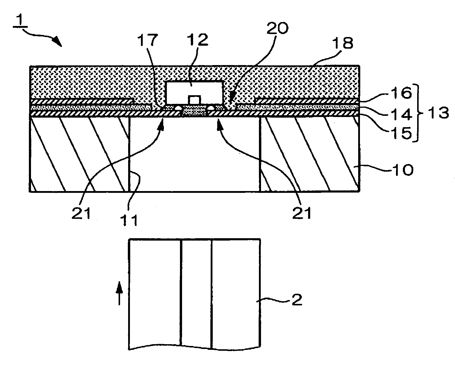
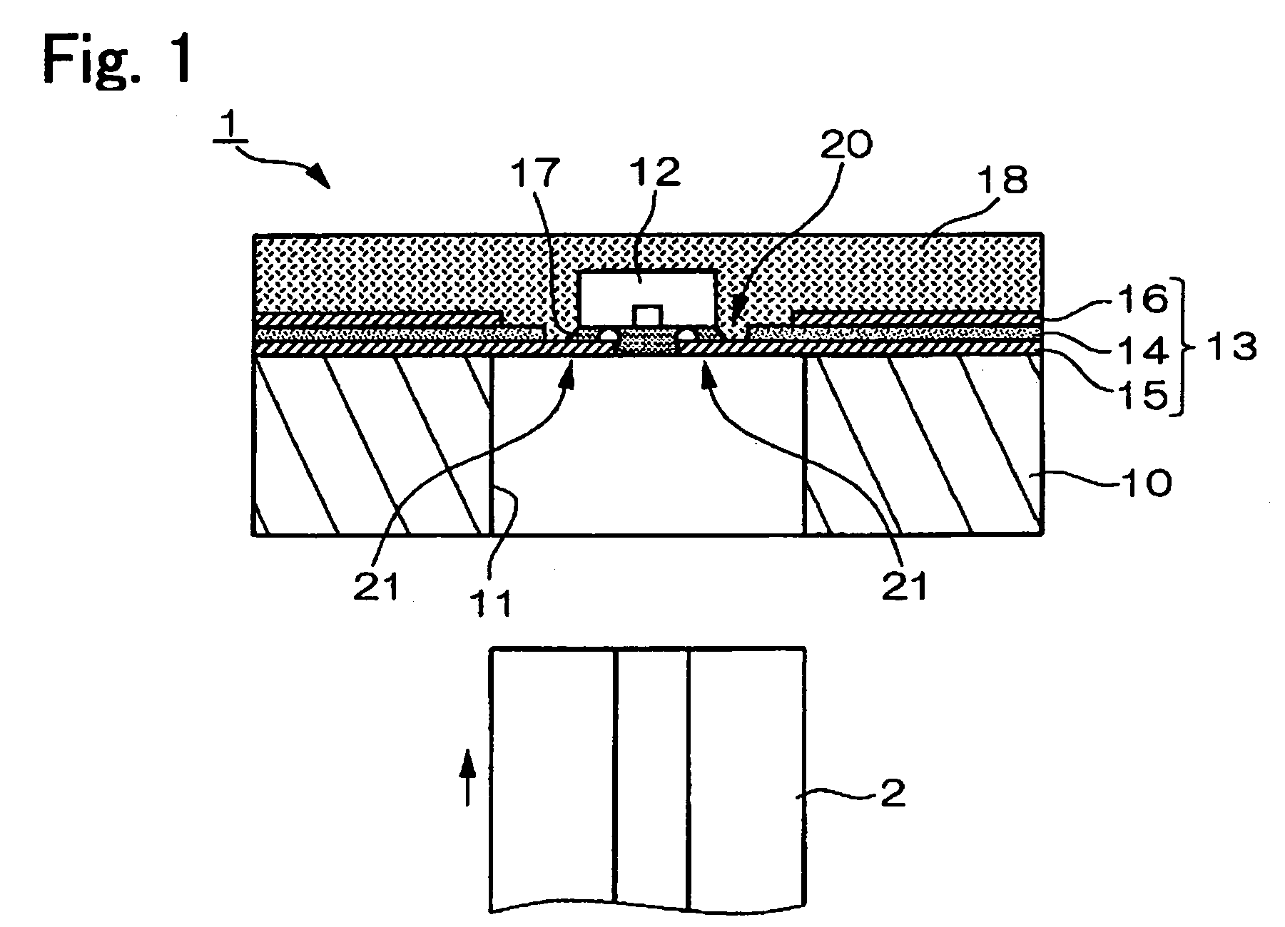
[0043]FIG. 1 is a schematic r explaining a structure of an optical module according to a first exemplary embodiment of the present invention. A cross-sectional view of the optical module according to the present embodiment is shown in the figure. An optical module 1 shown in FIG. 1 includes a substrate 10, an optical element 12, a flexible printed circuit board 13, an underfill member 17, and a sealing member 18. The optical module 1 is configured, as shown in the figure, so that an optical fiber 2 is detachably inserted in an aperture 11 provided in the substrate 10.

[0044]The substrate 10 supports each of the elements forming the optical module 1, and is equipped with the aperture 11 in which the optical fiber 2 is inserted. The substrate 10 can be made of various materials including conductive materials, such as stainless steel, aluminum, or cupper or nonconductive materials, such as glass, resin, or ceramics. In the present exemplary embodiment, the su...

second exemplary embodiment

(Second Exemplary Embodiment)

[0067]FIGS. 3a and 3b are schematics explaining a structure of an optical module according to a second embodiment. In the figure, a cross-sectional view of the optical module according to the present exemplary embodiment is illustrated. In the optical module 1a shown in the figures, the same reference numerals are used for the components that are common to the optical module 1 according to the first exemplary embodiment. The detailed description for the common components is omitted herein.

[0068]The optical module 1a shown in FIG. 3a includes a substrate 10a, the optical element 12, the flexible printed circuit board 13, the underfill member 17, and a sealing member 18a. The optical module 1a, for example, as shown in FIG. 3b, performs transmission or reception of the optical signal to or from the outside through a light guide 3 disposed on the other surface of the flexible printed circuit board 13. Alternatively, the optical module 1a can be used in comb...

third exemplary embodiment

(Third Exemplary Embodiment)

[0082]FIG. 5 is a schematic explaining a structure of an optical module according to the third exemplary embodiment. In the figure, a cross-sectional view of the optical module according to the present exemplary embodiment is illustrated. In the optical module 1b shown in the figure, the same reference numerals are used for the components that are common to the optical module 1 according to the first exemplary embodiment. The detailed description for the common components is omitted herein.

[0083]The optical module 1b shown in the figure is equipped with basically the same components as the optical module 1 according to the first exemplary embodiment as described above. The major difference is that the aperture 11 in which the optical fiber 2 is inserted is omitted. More specifically the optical module 1b includes a transparent substrate 10b, the flexible printed circuit board 13, the underfill member 17, and a sealing member 18b. This optical module 1b is...


PUM


Abstract

The invention provides an optical module that can reduce its cost. An optical module to which an optical fiber is detachably inserted, includes: a substrate with an aperture to which the optical fiber is inserted; a flexible printed circuit board disposed on one surface of the substrate and including: a base member with an opening in a corresponding location to the aperture; an interconnection layer disposed on at least one surface of the base member); and a connection section including a part of the interconnection layer exposed through the opening; and an optical element disposed within the opening of the flexible printed circuit board, and connected to the connection section, the optical element performing one of transmission and reception of an optical signal with the optical fiber.

Description

BACKGROUND OF THE INVENTION[0001]1. Field of Invention[0002]The present invention relates to an optical module suitable for application to optical communication systems, and to a manufacturing method of the optical module.[0003]2. Description of Related Art[0004]Related art optical communication systems have basic configurations, in which light emitting elements to convert an electrical signal to an optical signal and light receiving elements to convert an optical signal to an electrical signal, are connected through optical fibers. In order to detachably connect such optical elements as light emitting elements or light receiving elements with optical fibers, optical modules to optically connect optical elements to optical fibers are used. Such optical modules are described in various documents, such as Japanese laid-open patent publication No. 2000-349307, for example.SUMMARY OF THE INVENTION[0005]Since the optical modules mentioned above have structures in which substrates are int...

Claims


Application Information

Patent Timeline
Patent Type & Authority Patents(United States)
IPC IPC(8): G02B6/36G02B6/42G02B6/43H01L31/0232H01S5/022
CPCG02B6/4212G02B6/4214G02B6/4231G02B6/43H01L24/97H01L2224/32225H01L2224/83001H01L2224/73204H01L2224/16225H01L2924/00H01L2924/12042H01L2924/12043H01L2924/00014H01L2224/0401
Inventor MIYAMAE, AKIRANAGASAKA, KIMIO
Owner SEIKO EPSON CORP
Learn More