Torsion spring probe contactor design

a technology of contactors and springs, applied in the field of probe contactors, can solve the problems of design limitations, too long cantilever wire probes, and difficult to accurately assemble, and achieve the effect of high contras

Active Publication Date: 2008-04-22
FORMFACTOR INC
View PDF31 Cites 11 Cited by
  • Summary
  • Abstract
  • Description
  • Claims
  • Application Information

AI Technical Summary

Benefits of technology

[0018]Utilizing the manufacturing processes described in U.S. patent application Ser. Nos. 11 / 019,912 and 11 / 102,982, the present invention includes several novel features not present in the prior art. One of the novel features of the present invention is that the arm portion is in a different planar layer than the torsion bar and may be separated from the torsion bar by a spacer. The addition of these two added layers provides for greater design flexibility towards controlling the path of motion of the tip when it is actuated by a largely vertical force when testing a device. The availability of additional layers of the probe in this respect is made possible by the new manufacturing processes described in the above patent applications. In fact, as described, the torsion probe has at least eight planar layers utilized in the construction of the torsion contactor spring and these layers afford design flexibility to optimize the operational characteristics of the contactor while accommodating the process limitations imposed by commercially viable photolithographic micro-electro-forming techniques. The torsion probe may have more or fewer layers than eight without departing from the spirit of this invention.
[0019]The arm of the probe is also made more rigid than the torsion bar so that it does not act as a spring (as in a cantilever beam spring). If the bar was not rigid, its deformation would increase the scrub length beyond that which may be desired. The arm provides a lever which, in consort with the stop, transforms the largely linear arc of the tip to a nearly pure-torsion rotation of the torsion bar. In another embodiment, the arm is composed of two subarms, one extending from the top of the end of the other. This approach allows a greater clearance between the closest part of the spring structure and the wafer under test. Additional clearance helps to avoid damage to the wafer from foreign particles that may become caught between the probe structures and the wafer in the contacted state.
[0020]Another novel aspect of the present invention is that a stop is attached to the substrate and incorporates a lateral support to laterally support the torsion bar when it engages the stop. The basic function of the stop is to act as a fulcrum or pivot for the torsion bar. The lateral support provides an increase in lateral stability and more control over the tip's scrub pattern.
[0022]A further refinement is to provide a rough plated skirt that covers not only the top surface of the support post, but also wraps around the base of the tip. This construction not only creates a high contrast between the tip surface and the post but also provides for mechanical support of the tip in the form of a thickening or gusset around its base. The gusset further protects the tip from mechanical failure at its base caused by lateral forces during use, which is particularly useful if the tip has a high aspect ratio (height to width or diameter). This skirt may also be plated in a pattern that slightly overhangs the post structure so that slight misalignments (e.g., due to lithography errors) do not result in the exposure of the smooth reflective surface in the shape of a crescent or edge at one side of the perimeter of the post.

Problems solved by technology

Furthermore, the chuck and the probe card mechanical mount may not be precisely parallel and flat, introducing further height variations which the probes must accommodate.
However, cantilever wire probes are too long and difficult to accurately assemble to allow reliable simultaneous contact to all of the chips on a conventional wafer.
Additionally, cantilever wire probes have high self and mutual inductance problems which do not make them good candidates for testing of high-speed devices.
These problems are exaggerated when they are used to test larger wafers.
Moreover, they are elongated and poorly supported in lateral directions at the contactor causing problems with controlled scrubbing of the contact pads.
Furthermore, probes that require a long spring length such as these have relatively poor electrical performance.
However these designs too, have their limitations.
The particular incarnations considered and contemplated by these patents do not address or solve many of the practical requirements for a spring probe contactor such as: range of motion, optical characteristics required for vision recognition, practical production means, requirements for high lateral stability of the contact tip in response to scrubbing forces to name a few.
High contact force is deleterious to the semiconductor devices under test which often include active devices under the I / O pads.
Furthermore, pin based contactors cannot be built at the fine pitches and high pin counts required for modern large wafer test.
Typical microfabricated spring contactors have smooth planar surfaces in close proximity to the contact tip surface, creating difficulty with regard to the vision recognition systems due to reflections from surfaces other than the tip, as seen in FIG. 5A.
Thus, these vision systems often mistake unrelated structures for the tip causing vision rejections or errors in the captured tip position.
Various attempts to overcome this problem have been suggested, but each have had their own problems.
This extra bonding step adds significant complexity, yield loss, and cost to the manufacturing process.
Furthermore, the pyramid shape produces a contact geometry that is limited to a square or rectangular contact surface which grows in size as it is abraded or resurfaced as is often done in practical application as a result of abrasive cleaning.
However, this is not a practical solution for tips that are produced by lithographic imaging and electroforming.
Such processes have practical limits in aspect ratio (height to width ratio).
Furthermore, even if the aspect ratios of a taller tip were practical (typical tips are about the same height as or slightly higher than their smallest dimension which is on the order of 5 um to 20 um), a taller tip would be prone to breakage from the lateral scrubbing forces present in use.
However, a problem with this design is that it is very difficult to align a tip on the flat top of the now tapered post.
The crescent effect interferes with proper tip-position recognition causing vision “rejects” or errors in the captured visual centroid.

Method used


Image

  • Torsion spring probe contactor design
  • Torsion spring probe contactor design
  • Torsion spring probe contactor design

Examples


Embodiment Construction

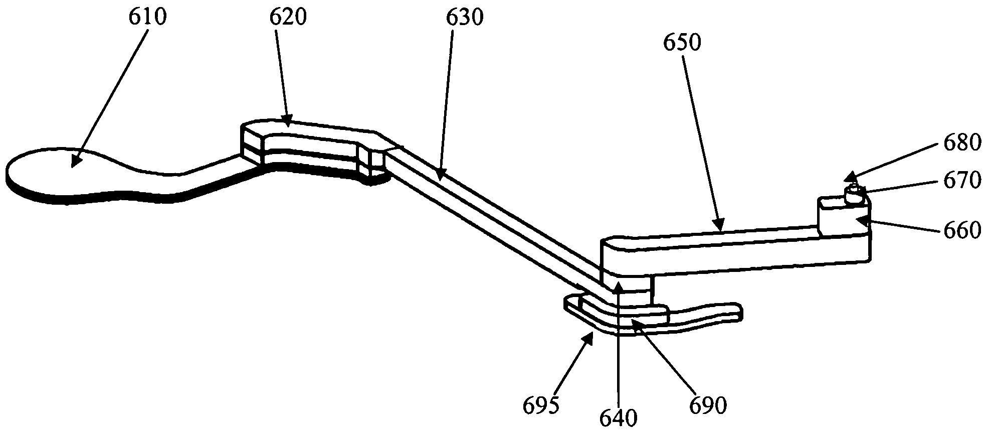
[0042]FIG. 6A shows a probe for testing an electronic device in accordance with an embodiment of the present invention. This embodiment of the probe incorporates a substrate 600, a trace layer 610, a foot element 620, a torsion bar 630, a spacer element 640, an arm 650, a post 660, a secondary post 670, a tip 680, and a stop element 690. Plated on a substrate 600 is a trace layer 610 providing an electrically conductive path from the foot 620 to a via 900 (see FIG. 9) in the substrate 600. This trace layer 610 may be electroplated gold having a nominal height (also termed thickness) of 16 um. The foot 620 provides the mechanical anchor for the probe. The foot 620 has both a proximal end (the end closest to the via 900) and a distal end (the end furthest from the via 900). The foot 620 is connected to a torsion bar 630 at its distal end. The torsion bar 630 is the element which provides the probe with its spring like (or compliant) qualities because when it is in an actuated state (i...


PUM


Abstract

The present invention relates to a probe for making electrical connection to a contact pad on a microelectronic device. A foot having a length, a thickness, a width, a proximal end, and a distal end, is connected to a substrate. The length of the foot is greater than its width. A torsion bar having a length, a width, a thickness, a proximal end, and a distal end, is connected to the distal end of the foot at the proximal end of torsion bar. The torsion bar lies in a first plane. A spacer having a length, a width, and a thickness, is connected to the distal end of the torsion bar. An arm having a length, a width, a thickness, a proximal end, and a distal end is connected to said spacer at the arms proximal end. The arm lies in a second plane and the second plane is in a different plane than the first plane. A first post having a top side and a bottom side is connected to the arm near the distal end of the arm. A tip is electrically connected to the top side of the post.

Description

BACKGROUND[0001]The present invention relates generally to the testing of semiconductor chips, and specifically to the design of probe contactors for such testing prior to packaging.[0002]Typically, semiconductor chips are tested to verify that they function appropriately and reliably. This is often done when the semiconductor devices are still in wafer form, that is, before they are diced from the wafer and packaged. This allows the simultaneous testing of many chips at a single time, creating considerable advantages in cost and process time compared to testing individual chips once they are packaged. If chips are found to be defective, then when the chips are diced from the wafer, the defective ones can be discarded and only the reliable chips are packaged. It is an axiom then that the larger a wafer that may be reliably tested at a time, the more savings can be incurred in cost and process time.[0003]Generally, when performing wafer testing, a chuck carrying a wafer is raised to ...

Claims


Application Information

Patent Timeline
Patent Type & Authority Patents(United States)
IPC IPC(8): G01R1/073
CPCG01R3/00G01R1/06727G01R1/06738G01R1/073
Inventor KHOO, MELVINTEA, NIMISMAIL, SALLEHHSU, YANGTANG, WEILONGGARABEDIAN, RAFFI
Owner FORMFACTOR INC
Why Eureka
Try Eureka