Common word line edge contact phase-change memory

a phase-change memory and common word technology, applied in the direction of basic electric elements, electrical equipment, semiconductor devices, etc., can solve the problems of difficult incorporation of chalcogenide phase-change memory into cmos circuits, limited shrinking ratio, cross-sectional area,

Inactive Publication Date: 2008-04-29
MACRONIX INT CO LTD
View PDF8 Cites 127 Cited by
  • Summary
  • Abstract
  • Description
  • Claims
  • Application Information

AI Technical Summary

Benefits of technology

[0010]Another implementation of the method forms a bottom electrode by depositing a film of conducting material and then removing a portion of the conducting material. Conducting material not removed can have a width substantially equal to the first dimension. The second dimension may be determined by an etch process as already mentioned. A cross-sectional area of a contact formed by this implementation of the method can be substantially smaller than 4F2.
[0002]The present invention relates generally to semiconductor fabrication methods and, more particularly, to fabrication of a phase-change memory cell.

Problems solved by technology

It is known that chalcogenide phase-change memory is not easy to incorporate into a CMOS circuit because the chalcogenide material requires a relatively high current density to change its state.
This technique can reduce the cross-sectional area, but the shrinking ratio is limited by the spacer thickness.
The shrinkage ratio can be limited.
Thus, it can be difficult to scale down the chalcogenide parts in this fashion.
There can be additional problems once the pores are scaled down.
For instance, the uniformity of the pore-to-pore diameters can be poor.
Moreover, the small pores can place constraints on the chalcogenide deposition process since it will be more difficult to deposit materials into the tiny openings.
For example, in the context of pores formed using the process of the preceding paragraph, overhang of the spacer may partially or fully occlude the pore, further compromising the reliability of the deposition procedure.
If the bottoms of the pores receive poor bottom coverage, the electrodes beneath them may not be able to predictably change the phases of the chalcogenide parts.
If the phases are not repeatable when a given current is applied, the memory cell cannot reliably store data.
Another critical issue arises in aligning phase-change material with a contacting electrode.
Because of the large current densities involved, even relatively small misalignments can create large changes in current density that may adversely affect the ability to program phase-change memory cells.

Method used


Image

  • Common word line edge contact phase-change memory
  • Common word line edge contact phase-change memory
  • Common word line edge contact phase-change memory

Examples


Embodiment Construction

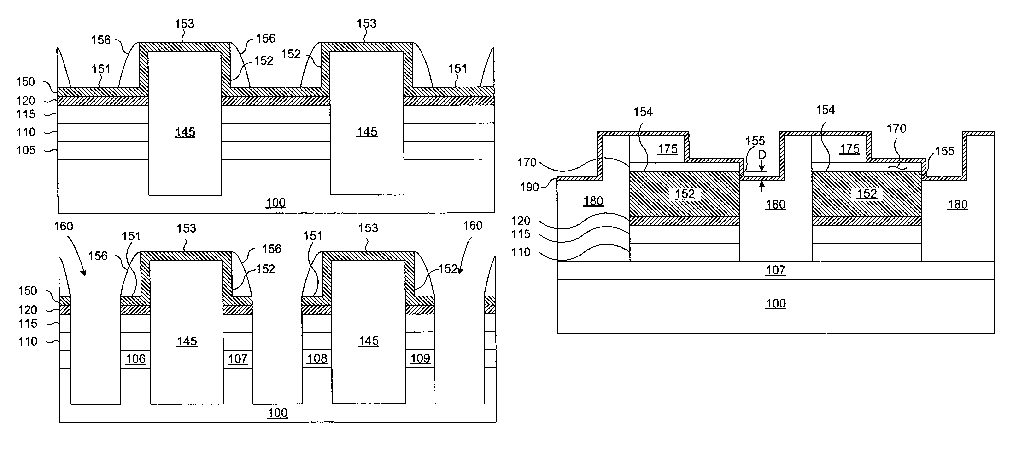
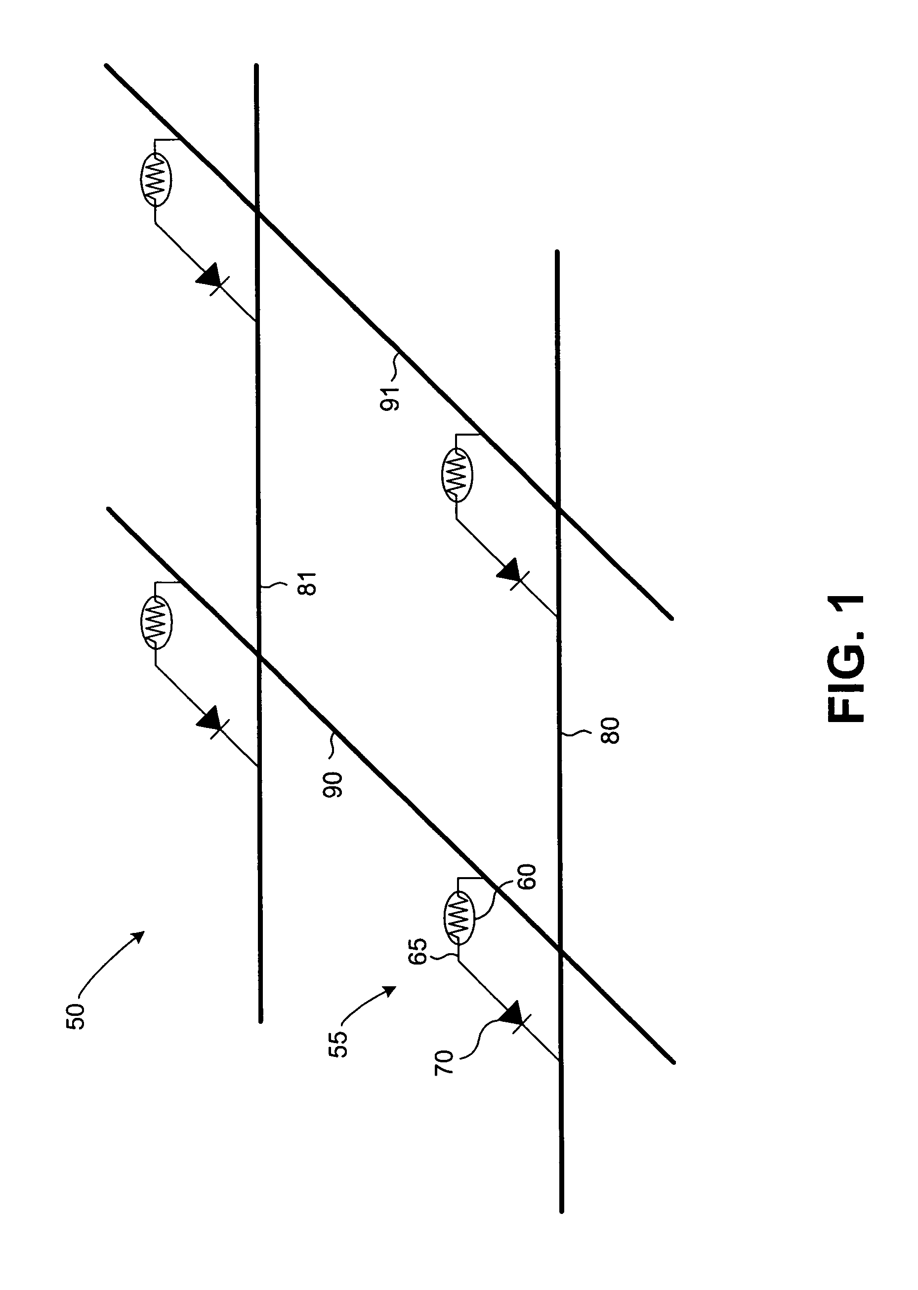
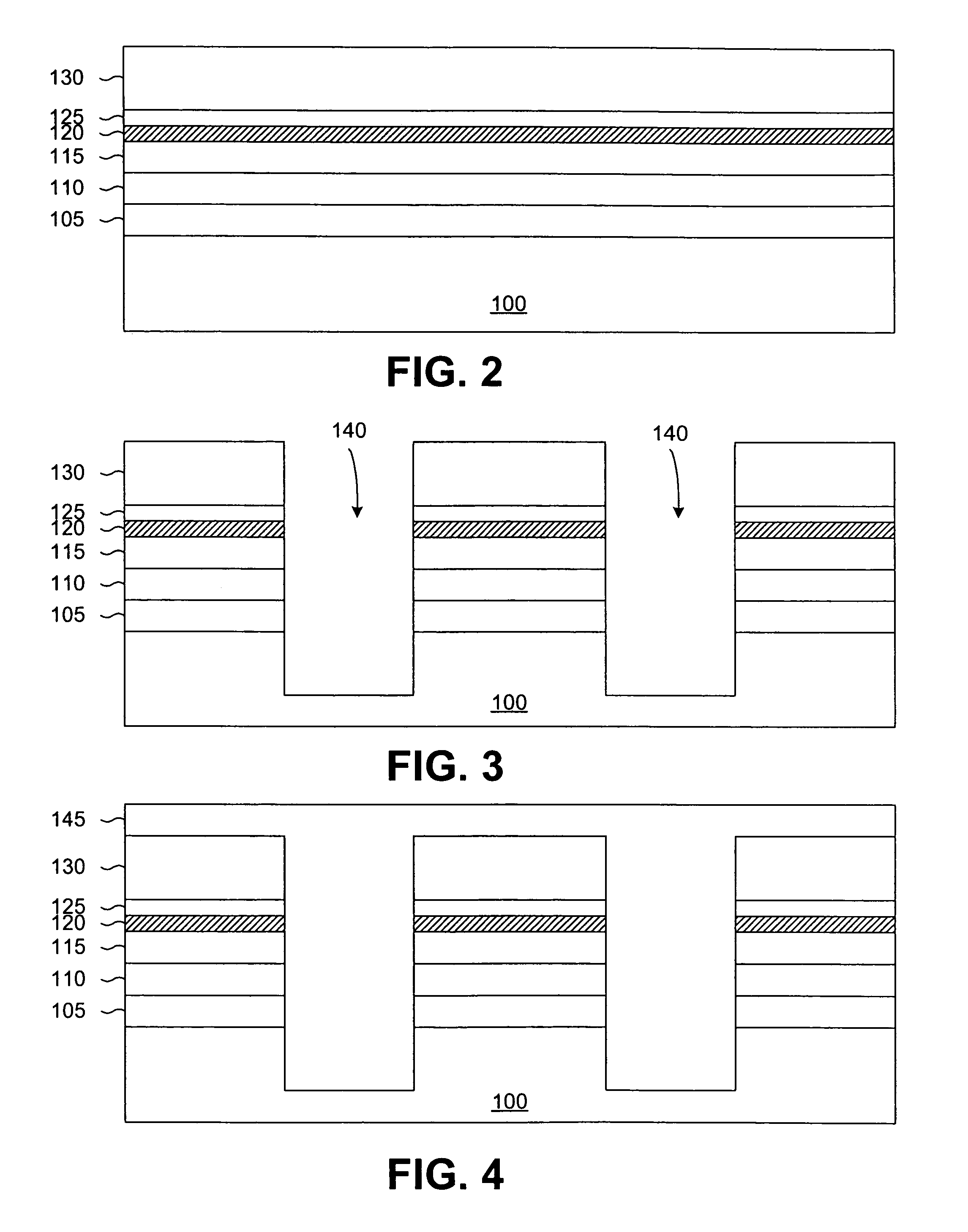
[0018]Reference will now be made in detail to the presently preferred embodiments of the invention, examples of which are illustrated in the accompanying drawings. Wherever possible, the same or similar reference numbers are used in the drawings and the description to refer to the same or like parts. It should be noted that the drawings are in simplified form and are not to precise scale. In reference to the disclosure herein, for purposes of convenience and clarity only, directional terms, such as, top, bottom, left, right, up, down, over, above, below, beneath, rear, and front, are used with respect to the accompanying drawings. Such directional terms should not be construed to limit the scope of the invention in any manner.

[0019]Although the disclosure herein refers to certain illustrated embodiments, it is to be understood that these embodiments are presented by way of example and not by way of limitation. The intent of the following detailed description, although discussing exe...


PUM


Abstract

A method of fabricating a phase-change memory cell is described. The cross-sectional area of a contact with a phase-change memory element within the cell is controlled by a first dimension of a bottom electrode and a second dimension controlled by an etch process. The contact area is a product of the first dimension and the second dimension. The method allows the formation of very small phase-change memory cells.

Description

BACKGROUND OF THE INVENTION[0001]1. Field of the Invention[0002]The present invention relates generally to semiconductor fabrication methods and, more particularly, to fabrication of a phase-change memory cell.[0003]2. Description of Related Art[0004]Electrically writable and erasable phase-change materials have traditionally been used for memory devices. Phase-change materials, which may be formed of chalcogenide materials, can be electrically switched between two structural states of generally crystalline and generally amorphous local order. The generally crystalline state is a phase in which the material's atoms and / or electrons form a repeatable lattice structure, whereas the atoms and / or electrons of the generally amorphous state are randomly distributed. The structural state can also be switched among a range of detectable structural states of local order between the extremes of completely crystalline and completely amorphous states.[0005]Currently favored chalcogenide materia...

Claims


Application Information

Patent Timeline
Patent Type & Authority Patents(United States)
IPC IPC(8): H01L21/44
CPCH01L45/06H01L45/1226H01L45/1273H01L45/141H01L27/2409H01L27/2463H10B63/20H10B63/80H10N70/823H10N70/231H10N70/8418H10N70/882
Inventor LUNG, HSIANG-LAN
Owner MACRONIX INT CO LTD
Why Eureka
Try Eureka