CMOS APS with stacked avalanche multiplication layer and low voltage readout electronics

a multiplication layer and low voltage readout technology, applied in the field of image sensors, can solve the problems of reducing the sensitivity of the image sensor, reducing the size of the electronic circuit in the device, and the potential for obtaining blurred images, so as to achieve the effect of reducing the problem of high voltag

Inactive Publication Date: 2008-04-29
APTINA IMAGING CORP
View PDF16 Cites 14 Cited by
  • Summary
  • Abstract
  • Description
  • Claims
  • Application Information

AI Technical Summary

Benefits of technology

[0008]The present invention mitigates problems of the high voltages which may be generated by a HARP layer under bright light conditions by incorporating a protection circuit into the pixel circuit connected to the HARP layer. The protection circuit prevents the pixel circuit from breaking down when the voltage in the pixel circuit reaches the operating voltage applied to the charge multiplying photoconversion layer in response to the image sensor being exposed to a strong light. In particular, the protection circuit of the present invention may be designed in any of several configurations in which additional voltage entering the pixel circuit from the charge multiplying photoconversion layer over a predetermined threshold voltage level is dissipated before reaching the storage node and other lower voltage components downstream therefrom.

Problems solved by technology

Due to the interior space constraints in the housings of the compact designs, it is necessary to reduce the sizes of the electronic circuits in the device, including the image sensor.
However, upon shrinking the size of the image sensor, a tradeoff must be made between resolution and the signal levels outputted from the image sensor.
Smaller pixels reduce the amount of charge that can be collected by each pixel during image exposure, which in turn reduces the sensitivity of the image sensor.
Although the reduced sensitivity effect can be offset by increasing the integration (exposure) time, this is an undesirable “solution” because increasing integration time also increases the potential for obtaining a blurred image if there is any movement by the image subject or the device during exposure.
On the other hand, in order to maintain the same sensitivity without having to increase integration time, the pixels must be made larger, which limits the resolution.
Thus, voltages of 50-100 V may be applied to the storage diode when the image sensor is exposed to a strong light, resulting in a breakdown of the readout components of the pixel circuit.
The double drain MOS transistor structure was shown to achieve an endurance voltage up to just under 60 V. However, a special MOS fabrication process is required for forming the double drain MOS transistor, and the size of the MOS transistor makes it difficult to attain small pixel sizes for high resolution image sensors.

Method used


Image

  • CMOS APS with stacked avalanche multiplication layer and low voltage readout electronics
  • CMOS APS with stacked avalanche multiplication layer and low voltage readout electronics
  • CMOS APS with stacked avalanche multiplication layer and low voltage readout electronics

Examples


first embodiment

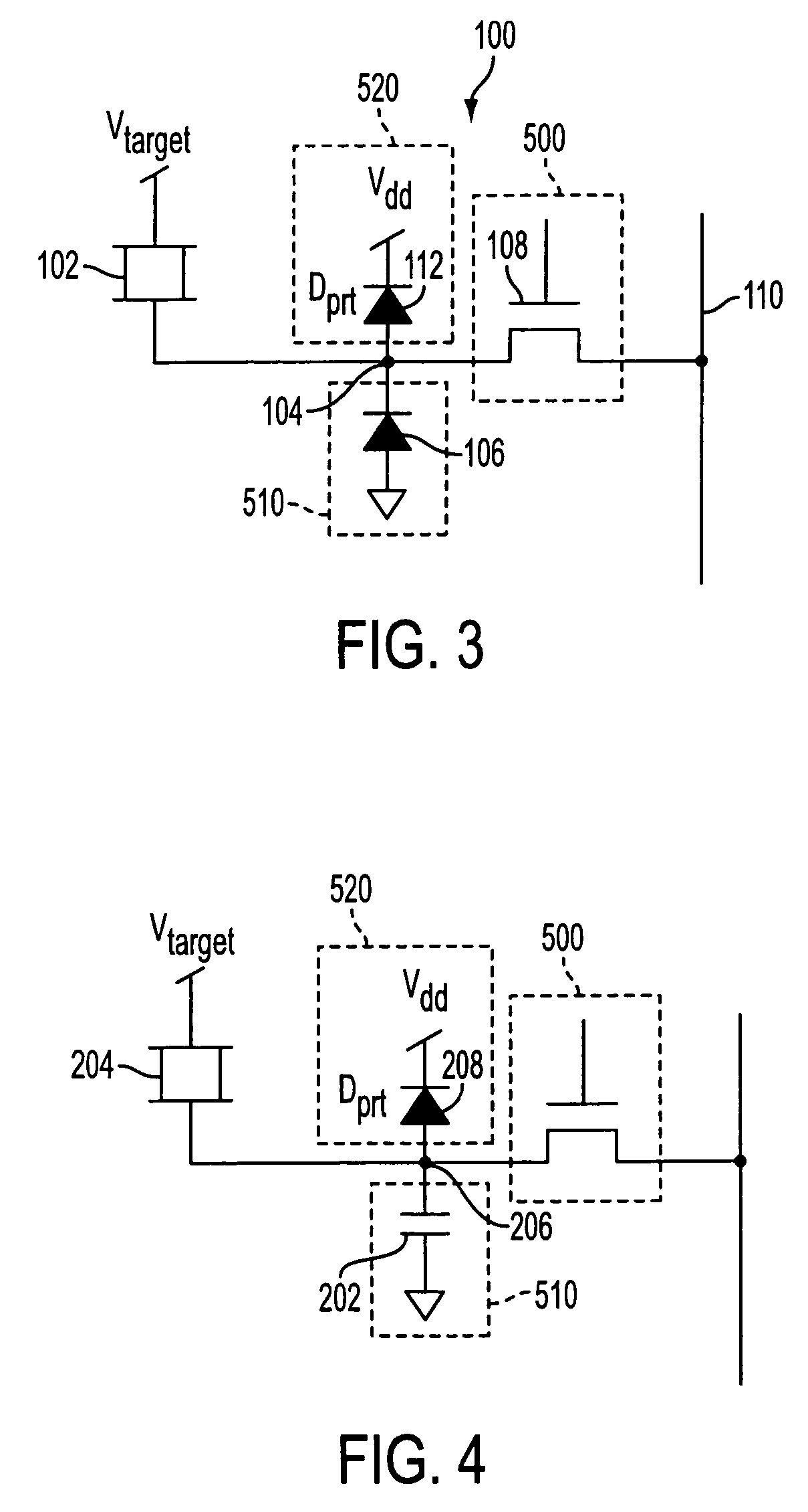
[0027]A second preferred embodiment of the present invention is shown in FIG. 4, and is identical to the pixel circuit of the first embodiment except that the storage element 510 is embodied as a storage capacitor 202 instead of a storage diode. Preferably, storage capacitor 202 has a large capacitance value per unit area, even more preferably in the range of 2-5 fF / μ2. Such a capacitor provides a higher capacitance value while reducing the space required for the charge storage region, relative to the use of a storage diode.

[0028]In this embodiment, charge from the charge multiplying photoconversion layer 204 is stored in the capacitor 202, until the voltage at the capacitor 206 reaches Vdd. Additional voltage flowing to node 206 from the charge multiplying photoconversion layer 204 is then directed through the protection diode 208 of protection circuit 520 so that the charge stored in the capacitor 202 maintains a voltage of around Vdd.

[0029]A third preferred embodiment of the pres...

fifth embodiment

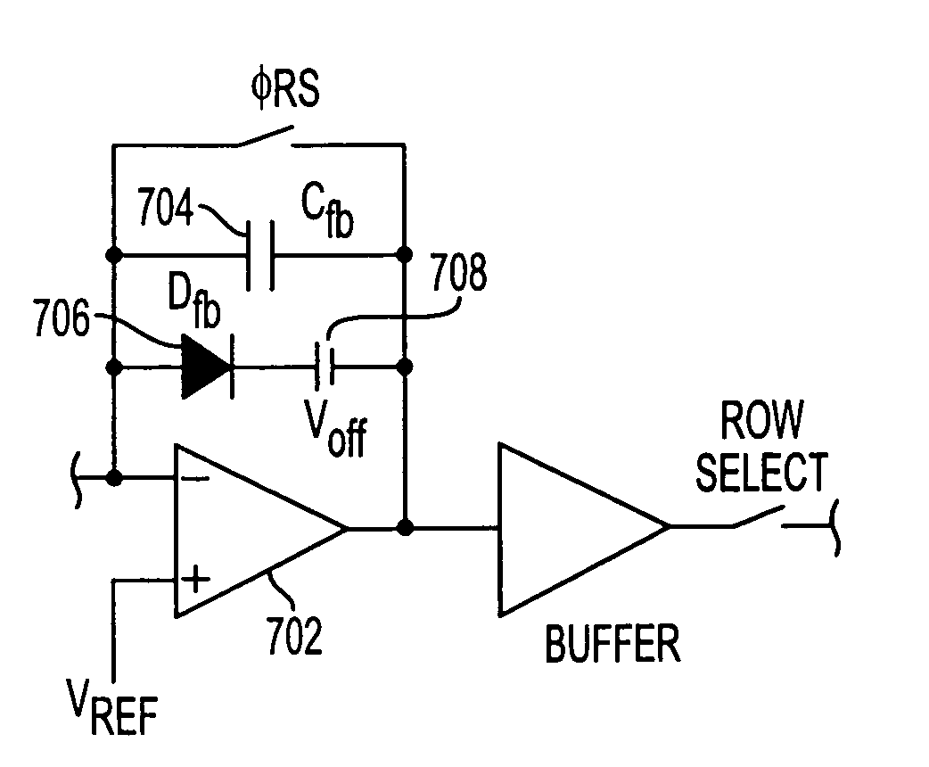
[0037]According to the present invention, as shown in FIG. 7, a differential amplifier 502 is connected to a constant voltage supply Vref at a positive input thereof, and the output is connected to a capacitor 504 in a feedback loop connecting to the negative input to the differential amplifier. A reset switch 506 is connected in parallel to the capacitor 504 between the negative input and the output of the differential amplifier 502 for shorting out the capacitor 504. A row select switch 508, which may be identical to the row select transistor 108 discussed above with reference to FIG. 3, is also connected to the output of the differential amplifier downstream of the connection to the capacitor 504.

[0038]During the integration time in this embodiment, hole current from the charge (hole) amplifying photoconversion layer is inputted to the negative input of the differential amplifier, through the differential amplifier and through the feedback loop. In this manner, the hole current f...

sixth embodiment

[0042]The output circuit is shown in FIG. 8, and is identical to the output circuit of FIG. 7, except that the output circuit of FIG. 8 converts the hole current from the charge amplifying photoconversion layer into a logarithmic signal, to account for the decreasing amplification level of the charge multiplying photoconversion layer due to the inverse relationship between the voltage level at the storage node and the effective Vtarget. In this regard, instead of a capacitor connected between the negative input and the output of the differential amplifier as shown in FIG. 7, the output circuit of FIG. 8 provides a feedback diode 604 having its anode connected to the negative input of the differential amplifier 602 and its cathode connected to the output of the differential amplifier 602. As configured in this manner, the output circuit of this embodiment thus logarithmically compresses the readout signal representing the intensity of the detected light.


PUM


Abstract

An image sensor includes a pixel having a protection circuit connected to a charge multiplying photoconversion layer. The protection circuit prevents the pixel circuit from breaking down when the voltage in the pixel circuit reaches the operating voltage applied to the charge multiplying photoconversion layer in response to the image sensor being exposed to a strong light. The protection circuit causes additional voltage entering the pixel circuit from the charge multiplying photoconversion layer over a predetermined threshold voltage level to be dissipated from the storage node and any downstream components.

Description

[0001]This application is a divisional of application Ser. No. 10 / 226,190, filed on Aug. 23, 2002, which is hereby incorporated by reference in its entirety.FIELD OF THE INVENTION[0002]The present invention relates to image sensors which use a stacked avalanche multiplication layer to amplify the intensity of light captured by a pixel circuit.BACKGROUND OF THE INVENTION[0003]Amid the rising popularity for digital image devices such as digital cameras is a demand for increasingly higher picture resolution and for increasingly compact designs of such devices. Due to the interior space constraints in the housings of the compact designs, it is necessary to reduce the sizes of the electronic circuits in the device, including the image sensor. However, upon shrinking the size of the image sensor, a tradeoff must be made between resolution and the signal levels outputted from the image sensor. If the resolution is kept the same upon reducing the size of the image sensor, the size of each p...

Claims


Application Information

Patent Timeline
Patent Type & Authority Patents(United States)
IPC IPC(8): H04N5/225H01L21/00H01L27/00H01L31/062H01L31/113H04N5/335H04N3/14G01J1/00G01T1/24H01J40/00H01L27/02H01L27/146H01L29/04H01L31/10H01L31/20H04N5/355
CPCH01L27/14643H04N3/1568H04N5/35518H04N5/35527H01L27/0251H01L27/14609H04N25/573H04N25/575H01L27/146H04N25/77
Inventor TAKAYANAGI, ISAONAKAMURA, JUNICHI
Owner APTINA IMAGING CORP
Why Eureka
Try Eureka