Unlock instant, AI-driven research and patent intelligence for your innovation.

Column sample-and-hold cell for CMOS APS sensor

Active Publication Date: 2008-04-29
APTINA IMAGING CORP
View PDF2 Cites 2 Cited by
  • Summary
  • Abstract
  • Description
  • Claims
  • Application Information

AI Technical Summary

Benefits of technology

[0015]The present invention provides an improved sample and hold readout circuit and method of operation which reduces fixed pattern noise during a read out operation. The circuit improves the consistency of the pixel to pixel output of the pixel array and increases the dynamic range of the pixel output. This is accomplished by eliminating the crowbar switch between the storage areas in the sample and hold circuit. Additionally, a switch is added further isolating the sample and hold circuit from the column line coupled to the pixel array. In this manner, the signals stored in the sample and hold circuit are transferred downstream by isolating the sample and hold circuit from the global column line and then using the sampling switches SH_R and SH_S to short the front plates of the capacitors together. This has the additional advantage of creating a more symmetrical sample and hold circuit.

Problems solved by technology

One issue associated with the APS CMOS imaging systems is that of fixed pattern noise, which is type of distortion in the image captured by the imaging system.
One source of fixed pattern noise is due to imperfections in the sample and hold circuit.
The layout of the sample and hold circuit contributes to the amount of fixed pattern noise.
Due to the delta sampling nature of the timing scheme, floating capacitor plates are still present in the circuit with a direct coupling to each other and this presents a detrimental effect for any further improvement to the sensor fixed pattern noise.

Method used


Image

  • Column sample-and-hold cell for CMOS APS sensor
  • Column sample-and-hold cell for CMOS APS sensor
  • Column sample-and-hold cell for CMOS APS sensor

Examples


Embodiment Construction

[0025]In the following detailed description, reference is made to the accompanying drawings, which form a part hereof, and in which is shown by way of illustration specific embodiments in which the invention may be practiced. These embodiments are described in sufficient detail to enable those of ordinary skill in the art to make and use the invention, and it is to be understood that structural, logical or other changes may be made to the specific embodiments disclosed without departing from the spirit and scope of the present invention.

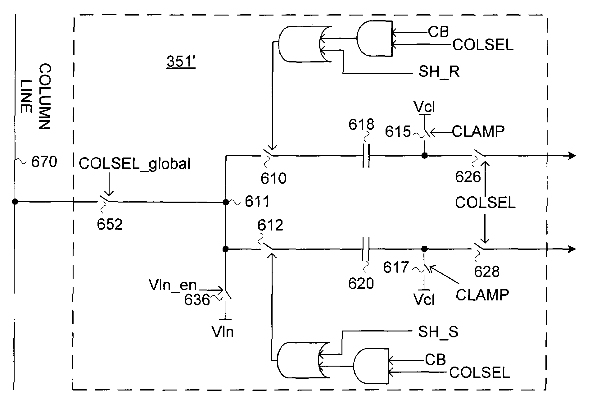
[0026]The present invention eliminates the crowbar switch and utilizes the sampling switches to short the front plates of the capacitors together when performing a read out from the sample and hold circuit.

[0027]An embodiment of the invention is shown and described with reference to FIGS. 6 and 7. The sample and hold circuit 351′ of FIG. 6 is different from the sample and hold circuit 351 of FIG. 4 in several respects: the crowbar 411 circuit includi...


PUM


Abstract

A sample and hold readout circuit and method of operation which minimizes fixed pattern noise during a read out operation. The circuit improves the consistency of the pixel to pixel output of the pixel array and increases the dynamic range of the pixel output. This is accomplished by eliminating the crowbar between the storage elements in the sample and hold circuit. Switches are added to isolate the sample and hold circuit from the column line coupled to the pixel array and to short the front plates of the capacitors together. Activating these switches allows the signals stored in the sample and hold circuit to be transferred downstream without the use of a crowbar switch.

Description

FIELD OF THE INVENTION[0001]The invention relates generally to semiconductor imaging devices and in particular to an imaging device which can be fabricated using a standard CMOS process. Particularly, the invention relates to a CMOS active pixel sensor (APS) imager having an array of pixel cells and to the column circuitry for reading the cells.BACKGROUND OF THE INVENTION[0002]There is a current interest in CMOS active pixel imagers for use as low cost imaging devices. An exemplary pixel circuit of a CMOS active pixel sensor (APS) is described below with reference to FIG. 1. Active pixel sensors can have one or more active transistors within the pixel unit cell, can be made compatible with CMOS technologies, and promise higher readout rates compared to passive pixel sensors. The pixel circuit of FIG. 1, designated generally by reference number 100, includes an exemplary pixel cell 150, which is a 3T APS cell, where the 3T is commonly used in the art to designate use of three transis...

Claims


Application Information

Patent Timeline
IPC IPC(8): H04N3/14H04N5/335H04N5/355H04N5/365H04N5/374H04N5/378
CPCH04N5/3575H04N5/3658H04N5/3745H04N25/616H04N25/677H04N25/77
Inventor ROSSI, GIUSEPPE
Owner APTINA IMAGING CORP