Differential readout from pixels in CMOS sensor

a pixel and pixel technology, applied in the field of cmos imagers, can solve the problems of affecting the final output of pixel signals, compromising the signal to noise ratio of image sensor cores, and breaking the equipotentiality of substrates, so as to improve the consistency of pixel to pixel output, improve the readout, and minimize substrate and other common mode noise

Active Publication Date: 2008-05-20
APTINA IMAGING CORP
View PDF20 Cites 13 Cited by
  • Summary
  • Abstract
  • Description
  • Claims
  • Application Information

AI Technical Summary

Benefits of technology

[0013]The present invention provides an improved pixel readout circuit and method of operation which minimizes substrate and other common mode noise during a read out operation. The circuit improves the consistency of the pixel to pixel output of the pixel array and increases the dynamic range of the pixel output. This is accomplished by obtaining a differential readout of the reset signal and integrated charge signal from a desired pixel along with a reset signal and a comparison signal from a different reference pixel, where the comparison signal is a reset signal taken in the reference pixel at the sam

Problems solved by technology

This increases substrate noise coupling to a pixel, which can compromise the signal to noise ratio of the image sensor core.
The substrate noise occurs when spurious noise signals are injected locally into the substrate through ohmic or capacitive coupling, thereby breaking the equipotentiality of

Method used


Image

  • Differential readout from pixels in CMOS sensor
  • Differential readout from pixels in CMOS sensor
  • Differential readout from pixels in CMOS sensor

Examples


Embodiment Construction

[0028]In the following detailed description, reference is made to the accompanying drawings, which form a part hereof, and in which is shown by way of illustration specific embodiments in which the invention may be practiced. These embodiments are described in sufficient detail to enable those of ordinary skill in the art to make and use the invention, and it is to be understood that structural, logical or procedural changes may be made to the specific embodiments disclosed without departing from the spirit and scope of the present invention.

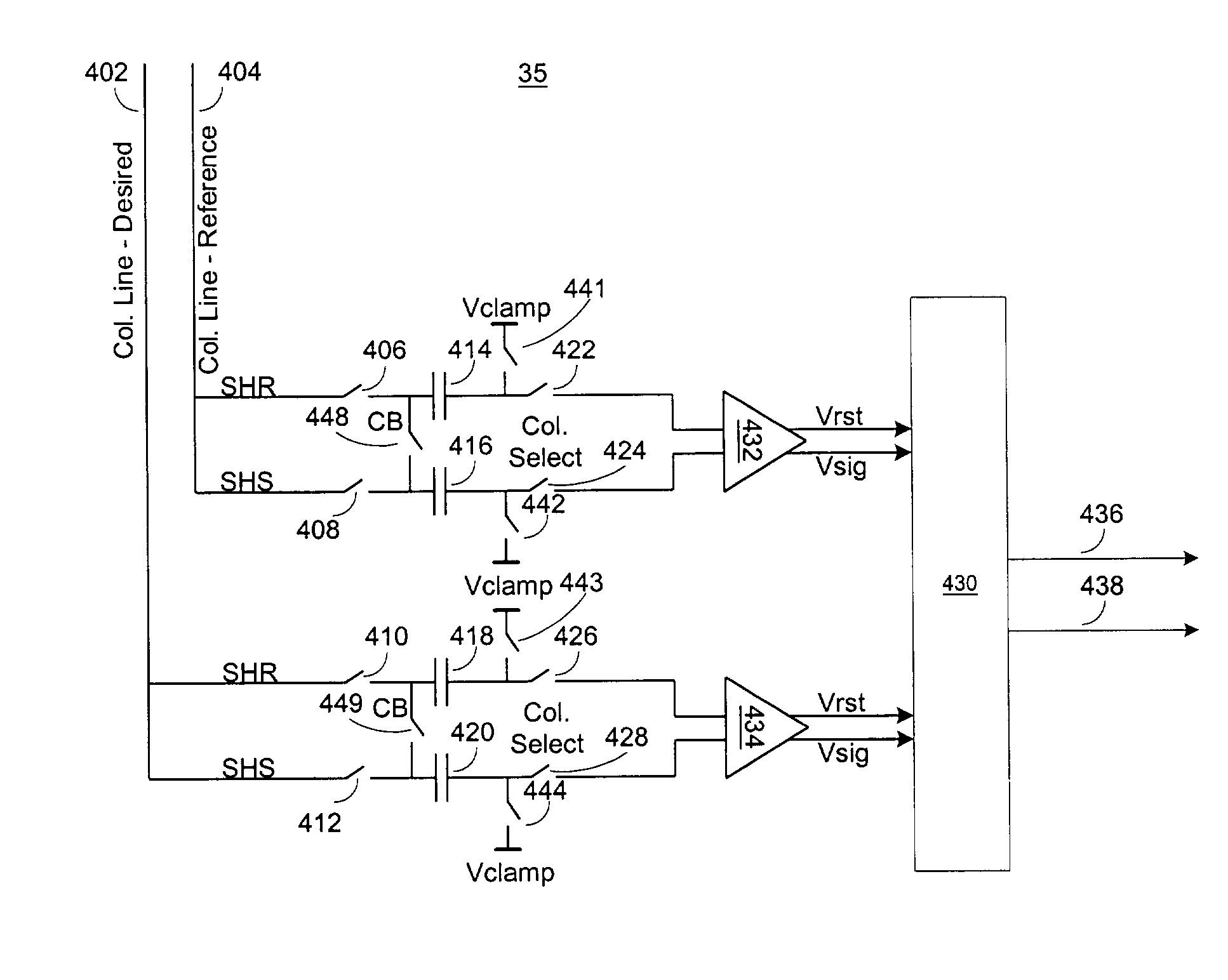
[0029]To minimize common ground noise and the loss of fill factor the present invention utilizes a neighbor pixel as the source of a reference differential signal which is combined with the output of a desired pixel. In an exemplary embodiment, the actual photosignal from the neighboring pixel is not read when the neighboring pixel acts as reference pixel, only a reference value is taken as a comparison signal from the reference pixel at the tim...


PUM


Abstract

The present invention provides an improved pixel readout circuit that compensates for common mode noise during a read out operation. This is accomplished by using a differential readout of the signal and reset value from the desired pixel compared with the reset value from a reference pixel. In this manner common mode noise can be offset and therefore minimized. In one embodiment of the invention, the reference pixel is the nearest neighbor pixel in the same row. In another embodiment, the reference pixel is the nearest neighboring pixel in a different row.

Description

FIELD OF THE INVENTION[0001]The invention relates generally to improved semiconductor imaging devices and in particular to an imaging device which can be fabricated using a standard CMOS process. Particularly, the invention relates to a CMOS imager having an array of image sensing cells and to the driving signals which operate the cells.BACKGROUND OF THE INVENTION[0002]There is a current interest in CMOS active pixel imagers for possible use as low cost imaging devices. An exemplary pixel circuit of a CMOS active pixel sensor (APS) is described below with reference to FIG. 1. Active pixel sensors can have one or more active transistors within the pixel unit cell, can be made compatible with CMOS technologies and promise higher readout rates compared to passive pixel sensors. The FIG. 1 exemplary pixel cell 10 is a 4T APS, where the 4T is commonly used in the art to designate use of four transistors to operate the pixel. A 4T pixel has a photodiode 162, a reset transistor 184, a tran...

Claims


Application Information

Patent Timeline
IPC IPC(8): H04N5/217H04N5/355H04N5/357H04N5/374H04N5/378
CPCH04N3/1512H04N3/1568H04N5/361H04N25/616H04N25/63H04N25/76H04N25/75
Inventor KRYMSKI, ALEXANDER
Owner APTINA IMAGING CORP
Why Eureka
Try Eureka