

Non-volatile semiconductor memory device with alternative metal gate material
a metal gate material and semiconductor technology, applied in semiconductor devices, instruments, electrical appliances, etc., can solve the problems of insufficient or sufficiently fast drop off of the threshold voltage vsub>th /sub> in known sonos devices, poor erase efficiency,
- Summary
- Abstract
- Description
- Claims
- Application Information
AI Technical Summary
Benefits of technology
Problems solved by technology
Method used
Image

Examples
Embodiment Construction
[0036]The present invention will now be described more fully with reference to the accompanying drawings, in which exemplary embodiments of the invention are shown. The invention may, however, be embodied in many different forms and should not be construed as being limited to the embodiments set forth herein; rather, these embodiments are provided so that this disclosure will be thorough and complete, and will fully convey the concept of the invention to those skilled in the art.
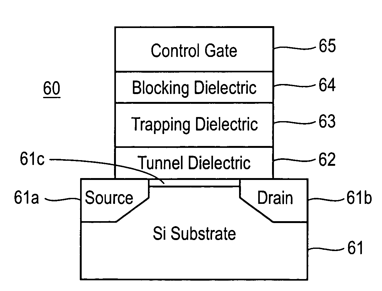
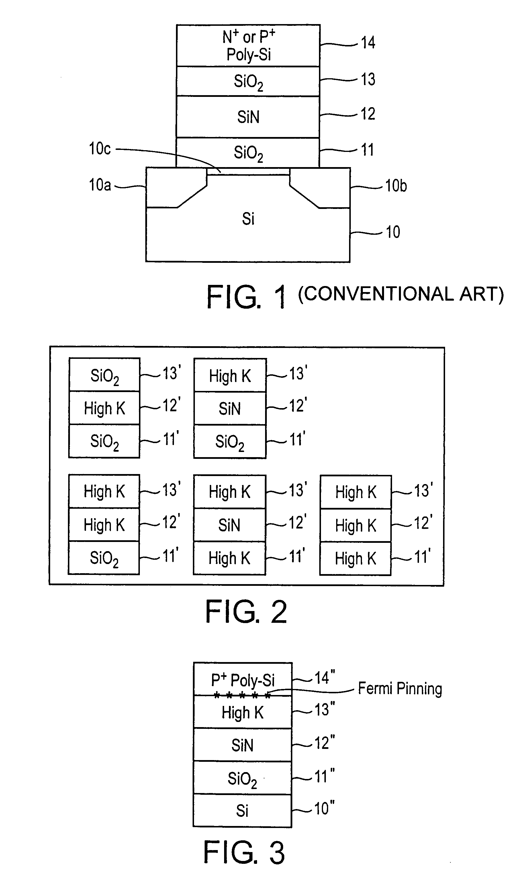
[0037]FIG. 5 illustrates a floating gate stack-type non-volatile memory 50, which includes a substrate 51 made of, for example, silicon. Other materials for the substrate 51 can be used, but silicon is currently the most common. In the substrate 51 are formed a source 51a and a drain 51b between which is formed a channel region 51c. It should be noted that, in this instance, the term “substrate” should be interpreted broadly to include wafers or other forms of substrates whether rigid or flexible, and also i...
PUM
 Abstract
Description
Claims
Application Information