Unit semiconductor chip and multi chip package with center bonding pads and methods for manufacturing the same

a technology of center bonding and semiconductor chips, which is applied in the direction of semiconductor devices, semiconductor/solid-state device details, electrical apparatus, etc., can solve the problems of electrical failure between, difficulty in conventional stacking process of manufacturing such a stacked semiconductor package, and overall thickness of the package, so as to reduce or prevent electrical failure

Active Publication Date: 2008-06-24
SAMSUNG ELECTRONICS CO LTD
View PDF14 Cites 162 Cited by
  • Summary
  • Abstract
  • Description
  • Claims
  • Application Information

AI Technical Summary

Benefits of technology

[0009]In an exemplary embodiment, the present invention provides a unit semiconductor chip with center bonding pads and at least one circuit layer to reduce the length of a bonding wire.
[0010]In another exemplary embodiment, the present invention provides a stacked semiconductor package with center bonding pads and at least one circuit layer to reduce the length of a bonding wire.
[0022]Various exemplary embodiments of the present invention may reduce or prevent electrical failures between the semiconductor chip and the bonding wires.

Problems solved by technology

Further, electrical failures may occur between an edge portion of the semiconductor chip 20 and the bonding wires 36, as a result of reducing the height of the wire loop to reduce the overall thickness of the package.
Furthermore, the conventional stacking process of manufacturing such a stacked semiconductor package may be difficult, as a result of sealing the top surface of the semiconductor chip 20 with the center bonding pads 25.

Method used


Image

  • Unit semiconductor chip and multi chip package with center bonding pads and methods for manufacturing the same
  • Unit semiconductor chip and multi chip package with center bonding pads and methods for manufacturing the same
  • Unit semiconductor chip and multi chip package with center bonding pads and methods for manufacturing the same

Examples


Embodiment Construction

[0030]The present invention will now be described more fully with reference to the accompanying drawings, in which exemplary embodiments of the invention are shown. It should be understood, however, that exemplary embodiments of the present invention described herein can be modified in form and detail without departing from the spirit and scope of the invention. Accordingly, the exemplary embodiments described herein are provided by way of example and not limiting, and the scope of the present invention is not restricted to the exemplary embodiments described herein.

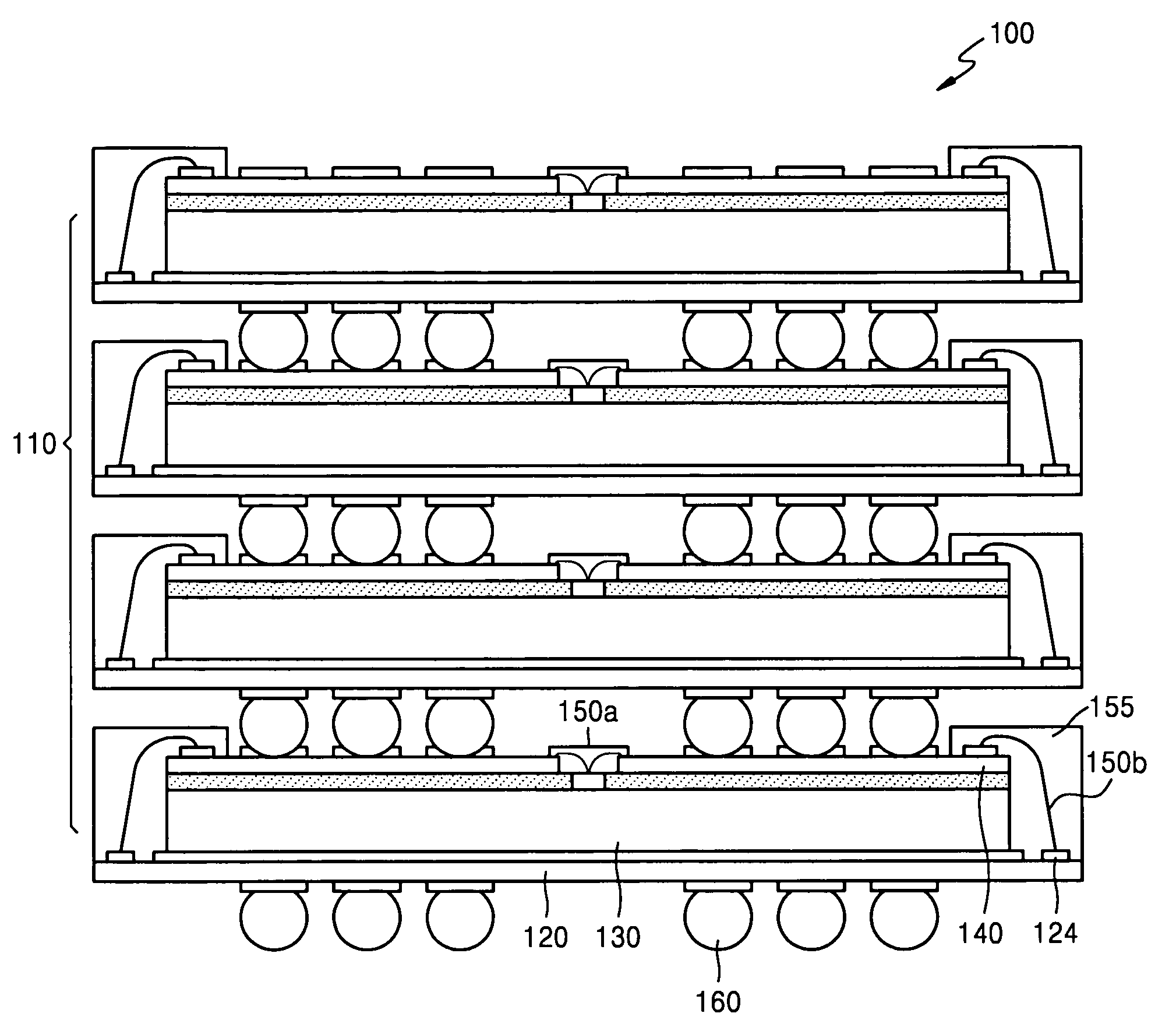
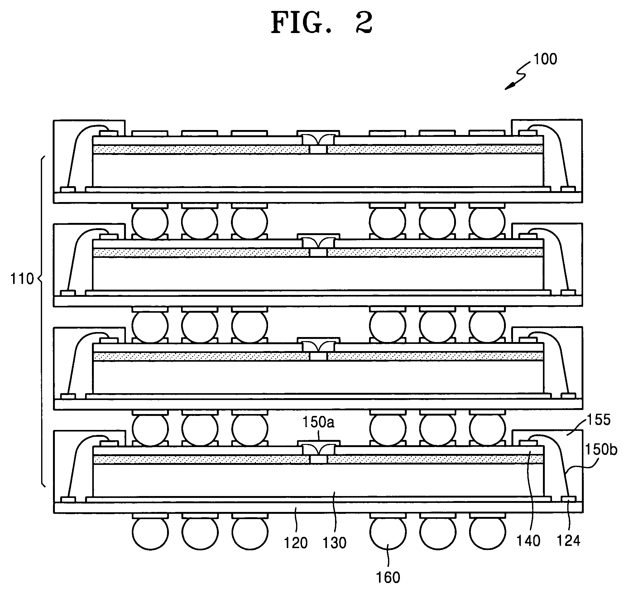
[0031]Referring to FIG. 2, according to an exemplary embodiment of the present invention, a stacked semiconductor package 100 may include at least one unit semiconductor package 110. The unit semiconductor package 110 may be the same or substantially similar to other unit semiconductor packages in the stacked semiconductor package 100. Referring to FIG. 3, the unit semiconductor package 110 may include a printed circuit ...


PUM


Abstract

A unit semiconductor chip and stacked semiconductor package and method of manufacturing with center bonding pads and at least one circuit layer to reduce the length of bonding. The unit semiconductor chip includes a first series of bonding wires connected to a plurality of center bonding pads of a semiconductor chip, at least one circuit layer connected to the first series of bonding wires and including a series of circuit layer wiring patterns, and a second series of bonding wires connecting the series of circuit layer wiring patterns and a series of wiring patterns. The stacked semiconductor package further includes a second series of wiring patterns, connected to the first series of wiring patterns, the a second series of wiring patterns and the series of circuit layer wiring patterns providing connections to adjacent lower and upper unit semiconductor packages, respectively.

Description

CROSS REFERENCE TO RELATED APPLICATIONS[0001]This application claims priority from Korean Patent Application No. 2003-59834, filed Aug. 28, 2003, the contents of which are hereby incorporated herein by reference in their entirety.BACKGROUND OF THE INVENTION[0002]1. Field of the Invention[0003]The present invention relates generally to a unit semiconductor chip, semiconductor package and methods for manufacturing the same. More particularly, the present invention relates to a unit semiconductor chip and a stacked semiconductor package having semiconductor chips with center bonding pads and methods for manufacturing the same.[0004]2. Description of Related Art[0005]As a result of developments in semiconductor technology and user demands, the electronic industry has been engaged in continuing efforts to reduce the size, thickness and power consumption of semiconductor devices. In order to meet the requirement of the electronic industry, semiconductor devices are becoming more highly in...

Claims


Application Information

Patent Timeline
Patent Type & Authority Patents(United States)
IPC IPC(8): H01L21/48H01L23/31H01L25/10H01L23/48
CPCH01L23/3128H01L25/105H01L2924/1815H01L2224/48091H01L2224/48227H01L2224/4824H01L2924/15311H01L2924/19107H01L2924/07802H01L2225/1023H01L2225/1041H01L2225/1058H01L24/48H01L2224/73265H01L2924/00014H01L2924/00H01L2924/14H01L2224/45099H01L2224/45015H01L2924/207H01L23/48
Inventor YEOM, KUN-DAE
Owner SAMSUNG ELECTRONICS CO LTD
Why Eureka
Try Eureka