Sheet-like probe, process for producing the same and its application

a technology of sheet-like probes and probes, applied in the field of sheet-like probes, can solve the problems of difficult in fact to stably and surely bring inspection probes of the probe device, the production of the probe device itself becomes difficult, and the positional deviation of the probe is prevented. , to achieve the effect of stably retaining a good electrical connection state and preventing positional deviation

Active Publication Date: 2008-06-24
ISC CO LTD
View PDF17 Cites 13 Cited by
  • Summary
  • Abstract
  • Description
  • Claims
  • Application Information

AI Technical Summary

Benefits of technology

[0017]The present invention has been made on the basis of the foregoing circumstances and has as its first object the provision of a sheet-like probe capable of surly preventing positional deviation between electrode structures and electrodes to be inspected by temperature changes in a burn-in test, even when the object of inspection is a wafer having a large area of 8 inches or greater in diameter or a circuit device, the pitch of electrodes to be inspected of which is extremely small, and thus capable of stably retaining a good electrically connected state.
[0018]A second object of the present invention is to provide a process capable of producing a sheet-like prove, by which in a burn-in test, positional deviation between electrode structures and electrodes to be inspected by temperature changes is surely prevented even when the object of inspection is a wafer having a large area of 8 inches or greater in diameter or a circuit device, the pitch of electrodes to be inspected of which is extremely small, and thus a good electrically connected state is stably retained.
[0019]A third object of the present invention is to provide a probe card capable of stably retaining a good electrically connected state in a burn-in test even when the object of inspection is a wafer having a large area of 8 inches or greater in diameter or a circuit device, the pitch of electrodes to be inspected of which is extremely small.

Problems solved by technology

When the circuit device to be inspected is a wafer, on which a great number of integrated circuits have been formed, it is however necessary to arrange a very great number of inspection probes upon production of a probe device for inspecting the wafer, so that such a probe device becomes extremely expensive.
In addition, when the pitch of electrodes to be inspected is small, the production of the probe device itself becomes difficult.
Further, since warpage generally occurs on wafers, and the condition of the warpage varies with individual products (wafers), it is difficult in fact to stably and surely bring inspection probes of the probe device into contact with a great number of electrodes to be inspected on the wafer, respectively.
However, such a sheet-like probe involves the following problems.
When a great difference in the absolute quantity of thermal expansion in a plane direction is caused between the wafer and the insulating sheet in the sheet-like probe as described above, it is difficult to surely prevent positional deviation between the electrode structures and the electrodes to be inspected by temperature changes in the burn-in test even when the peripheral edge portion of the insulating sheet is fixed by the holding member having a coefficient of linear thermal expansion equivalent to the coefficient of linear thermal expansion of the wafer, so that a good electrically connected state cannot be stably retained.
In addition, even when the object of inspection is a small-sized circuit device, it is difficult to surely prevent positional deviation between the electrode structures and the electrodes to be inspected by temperature changes in the burn-in test when a pitch between the electrodes to be inspected is 50 μm or less, so that a good electrically connected state cannot be stably retained.
However, in such a means, it is extremely difficult to evenly apply the tension to the insulating sheet in all directions of the plane direction thereof and a balance of the tension applied to the insulating sheet is changed by forming the electrode structures.
After all, the positional deviation between the electrode structures and the electrodes to be inspected by temperature changes cannot be prevented.
In addition, in order to fix the insulating sheet to the holding member in the state that the tension has been applied thereto, a complicated step of bonding the insulating sheet to the holding member under heating is required, so that a problem that increases in production cost is incurred arises.

Method used


Image

  • Sheet-like probe, process for producing the same and its application
  • Sheet-like probe, process for producing the same and its application
  • Sheet-like probe, process for producing the same and its application

Examples


example 1

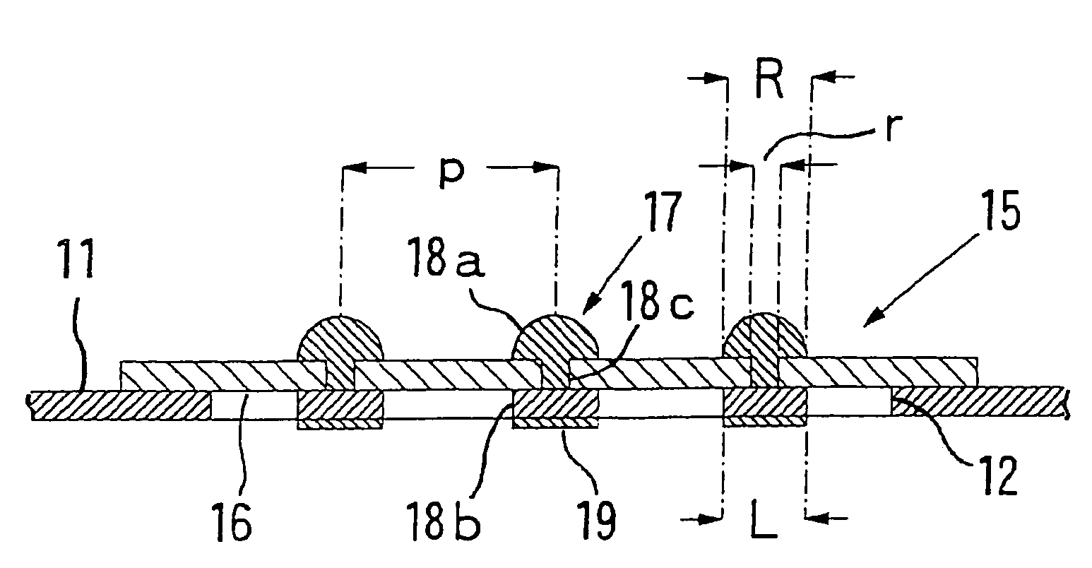
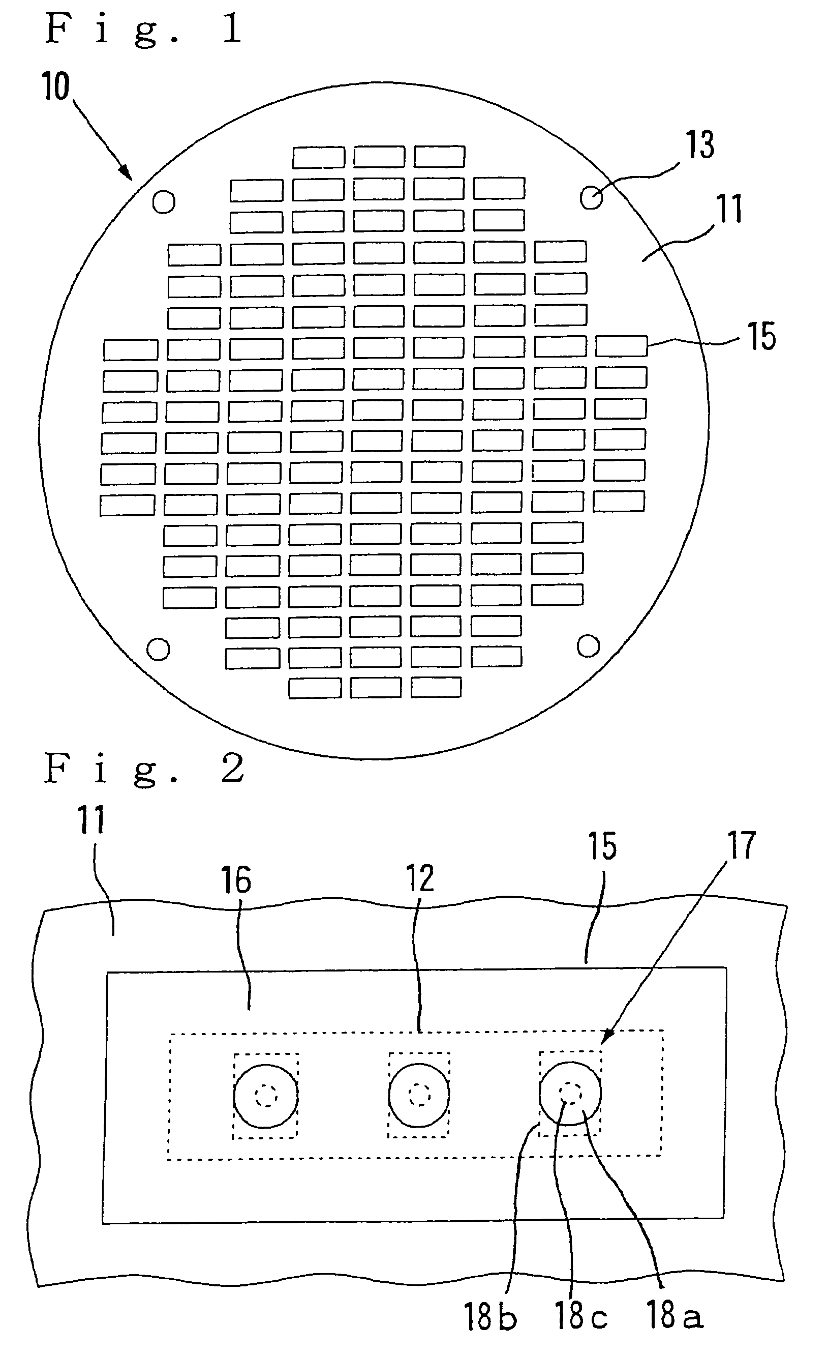
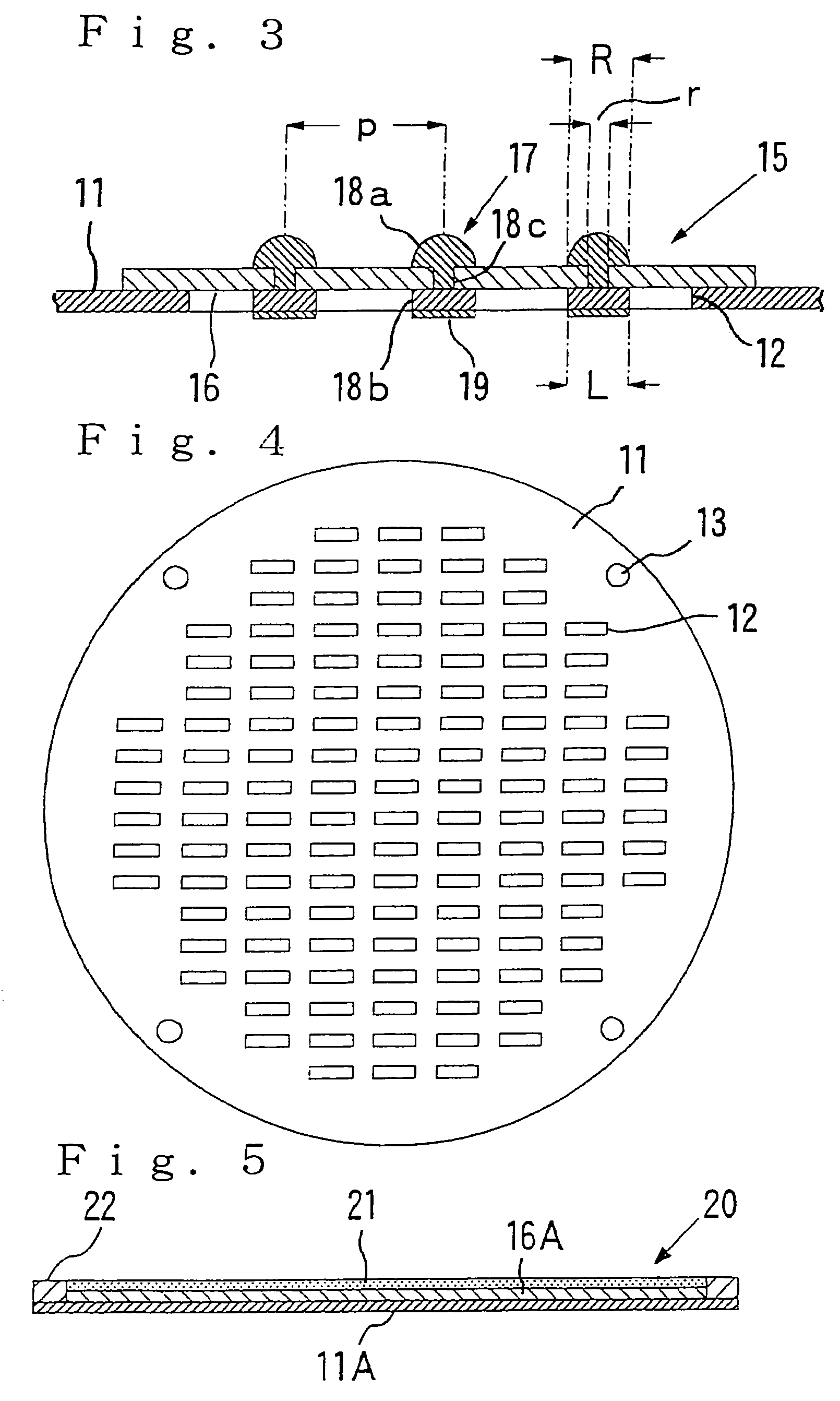
[0241]A laminated polyimide sheet with a copper layer having a diameter of 20 cm and a thickness of 5 μm laminated on one surface of a polyimide sheet having a diameter of 20 cm and a thickness of 12.5 μm and a laminated plate with a resin layer having a diameter of 20 cm and a thickness of 2.5 μm and composed of thermoplastic polyimide laminated on a surface of a metal plate having a diameter of 22 cm and a thickness of 25 μm and composed of 42 alloy were provided. The laminated polyimide sheet was then arranged on the surface of the resin layer of the laminated plate in such a manner that the polyimide sheet thereof faces the surface of the resin layer, and a protecting tape having an inner diameter of 20.4 cm, an outer diameter of 22 cm and a thickness of 25 μm and composed of polyethylene phthalate was arranged on a surface of a peripheral edge portion in the metal plate of the laminated plate. These were subjected to a pressure-bonding treatment under heat, thereby producing a ...


PUM


Abstract

Disclosed herein are a sheet-like probe capable of surly preventing positional deviation between electrode structures and electrodes to be inspected by temperature changes in a bum-in test, even when the object of inspection is a wafer having a large area of 8 inches or greater in diameter or a circuit device, the pitch of electrodes to be inspected of which is extremely small, and thus capable of stably retaining a good electrically connected state, and a production process and applications thereof. The sheet-like probe of the present invention comprises a contact film obtained by holding a plurality of electrode structures arranged in accordance with a pattern corresponding to respective electrodes to be connected and having a front-surface electrode part exposed to a front surface and a back-surface electrode part exposed to aback surface by an insulating film composed of a flexible resin, and a frame plate supporting the contract film.

Description

CONTINUING DATA[0001]This application is a 371 of PCT / JP04 / 06385, May 12, 2004.TECHNICAL FIELD[0002]The present invention relates to a sheet-like probe used in electrical inspection of circuit devices, and a production process and application thereof, and more particularly to a sheet-like probe suitable for use in conducting electrical inspection of, for example, a plurality of integrated circuits formed on a wafer in a state of the wafer, and a production process and applications thereof.BACKGROUND ART[0003]In electrical inspection of, for example, wafers, on which a great number of integrated circuits have been formed, or circuit devices of electronic parts such as semiconductor devices, a probe device having inspection electrodes arranged in accordance with a pattern corresponding to a pattern of electrodes to be inspected of a circuit device to be inspected is used. As such a probe device, may be used that, on which inspection electrodes (inspection probes) each composed of a pi...

Claims


Application Information

Patent Timeline
Patent Type & Authority Patents(United States)
IPC IPC(8): G01R1/073G01R31/02G01R3/00
CPCG01R1/0735G01R3/00H01L22/00G01R1/073
Inventor INOUE, KAZUOSATO, KATSUMI
Owner ISC CO LTD
Why Eureka
Try Eureka