Organic light emitting device and display device using the same

a technology of light emitting device and display device, which is applied in the field of display device, can solve the problems of unsatisfactory productivity, difficulty in dealing with a pixel that is smaller in size, and separate formation methods also have problems, so as to achieve high light emission efficiency, prevent accumulation of charges, and long life

Inactive Publication Date: 2008-07-15
SEMICON ENERGY LAB CO LTD
View PDF109 Cites 75 Cited by
  • Summary
  • Abstract
  • Description
  • Claims
  • Application Information

AI Technical Summary

Benefits of technology

[0073]The hole injection material and the electron injection material are capable of lowering the barrier in injecting carriers from electrodes to an organic compound film. Accordingly, the hole injection region and the electron injection region have an effect of making movement of carriers from the electrodes to the organic compound film smooth to prevent accumulation of charges. In order to avoid forming the impurity layer as described above, an injection mater

Problems solved by technology

However, the separate formation methods also have some problems.
For example, the shadow mask used in this method finds difficulties in dealing with a pixel that is smaller in size.
The operation of changing locations of the mask is rather onerous and leads to unsatisfactory productivity.
A more serious problem of the separate formation method is that, at present, characteristics (light emission efficiency and lifetime) vary between a red light emitting device, a green light emitting device, and a blue light emitting device.
On the other hand, the light emission efficiency of red light emitting device falls far below its required value.
Accordingly, under the present circumstances, low light emission efficiency of red light emitting device is the stumbling block to a full color display devic

Method used


Image

  • Organic light emitting device and display device using the same
  • Organic light emitting device and display device using the same
  • Organic light emitting device and display device using the same

Examples


embodiment 1

[0120]This embodiment shows a specific example of a device with a structure in which a hole injection region is inserted between an anode 501 and an organic compound film 502 in the blue organic light emitting device illustrated in FIG. 5A.

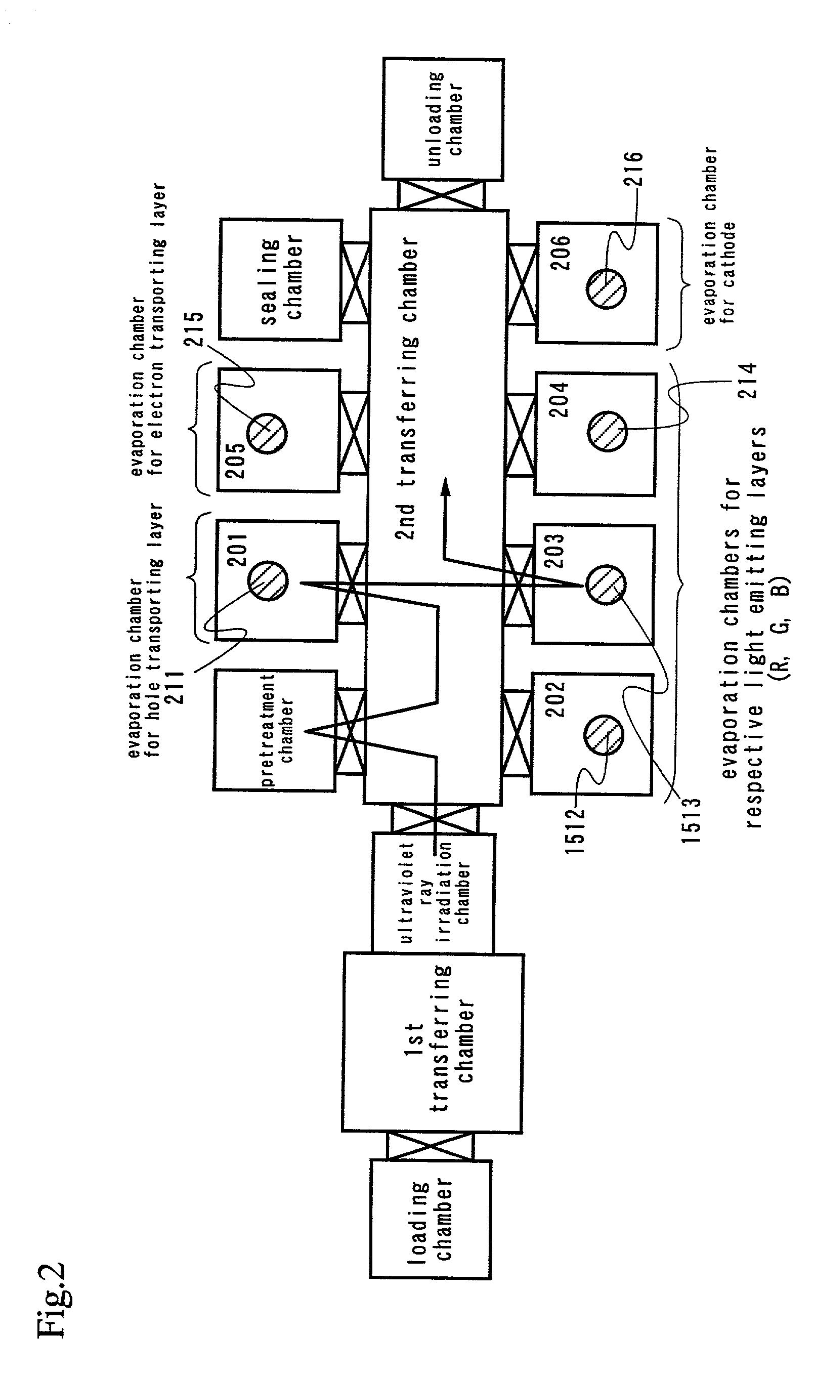
[0121]First, ITO is deposited to a thickness of about 100 nm by sputtering to form the anode 501 on the glass substrate 500. The glass substrate 500 having the anode 501 is brought into a vacuum tank as shown in FIGS. 11A and 11B. In this embodiment, five evaporation sources are necessary in order to deposit by evaporation five kinds of materials (four kinds of organic compounds and one kind of metal that forms the cathode).

[0122]First, MTDATA as a hole injection material is deposited by evaporation to a thickness of 20 nm to form a hole injecting region. When the film thickness reaches 20 nm and evaporation of MTDATA is ended, evaporation of spiro dimer of TAD (hereinafter referred to as S-TAD), that is a hole transporting material, is immediatel...

embodiment 2

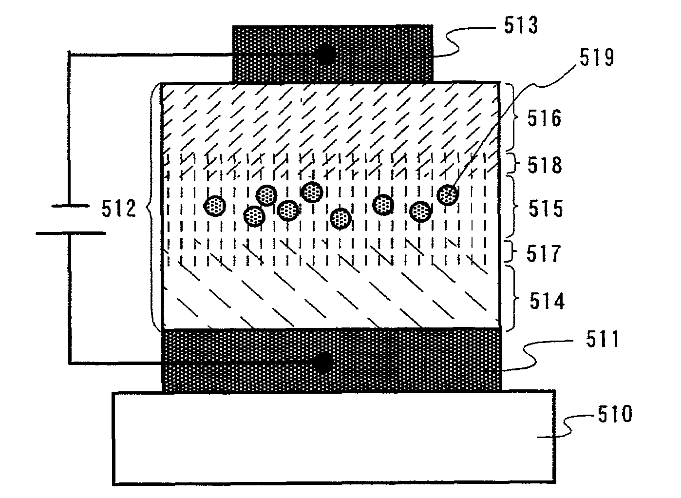
[0126]This embodiment shows a specific example of a device with a structure in which an electron injecting region is inserted between a cathode 513 and an organic compound film 512 in the blue organic light emitting device illustrated in FIG. 5B.

[0127]First, ITO is deposited to a thickness of about 100 nm by sputtering to form the anode 511 on the glass substrate 510. The glass substrate 510 having the anode 511 is brought into a vacuum tank as shown in FIGS. 11A and 11B. In this embodiment, six evaporation sources are necessary in order to deposit by evaporation six kinds of materials (five kinds of organic compounds and one kind of metal that forms the cathode).

[0128]First, the hole transporting region 514 consisting solely of TPD is formed to a thickness of 30 nm. Then, evaporation of BAlq as a host material to the light emitting material is started also at an evaporation rate of 3 Å / s with keeping the evaporation rate of TPD at 3 Å / s. In other words, the first mixed region 517 c...

embodiment 3

[0133]This embodiment shows a specific example of the white organic light emitting device illustrated in FIG. 6A.

[0134]First, ITO is deposited to a thickness of about 100 nm by sputtering to form the anode 501 on the glass substrate 500. The glass substrate 500 having the anode 501 is brought into a vacuum tank as shown in FIGS. 11A and 11B. In this embodiment, five evaporation sources are necessary in order to deposit by evaporation five kinds of materials (four kinds of organic compounds and one kind of metal that forms the cathode).

[0135]First, the hole transporting region 504 consisting solely of NPD is formed to a thickness of 30 nm. Then, evaporation of Zn(BTZ)2 as a blue light emitting material (actually the color is blueish white that is more white than blue) is started at an evaporation rate of 3 Å / s with keeping the evaporation rate of α-NPD at 3 Å / s. In other words, the first mixed region 507 containing α-NPD and Zn(BTZ)2 at a ratio of 1:1 is formed by coevaporation. The ...


PUM

PropertyMeasurementUnit
Efficiencyaaaaaaaaaa
Fluorescenceaaaaaaaaaa

Abstract

An organic compound film is composed of a hole transporting region, a first mixed region, a light emitting region, a second mixed region, and an electron transporting region that are connected to one another. With the organic compound film thus structured, the blue organic light emitting device obtained is free from interfaces between layers which are present in the conventional laminate structure. When pigment doping is added to this device structure, a white organic light emitting device is obtained. A blue or white organic light emitting device having high light emission efficiency and long lifetime is provided by this method. When this organic light emitting device is combined with color conversion layers or color filters, a full color display device that consumes less power and lasts long can be obtained.

Description

BACKGROUND OF THE INVENTION[0001]1. Field of the Invention[0002]The present invention relates to a display device using an organic light emitting device that has an anode, a cathode, and a film containing an organic compound that emits light by application of electric field (hereinafter referred to as organic compound film). Specifically, the present invention relates to a full color display device using a blue organic light emitting device or a white organic light emitting device that has higher light emission efficiency and longer lifetime than conventional ones. The term display device in this specification refers to an image display device that employs as a light emitting device an organic light emitting device. Also included in the definition of the display device are: a module in which a connector, such as an anisotropic conductive film (FPC: flexible printed circuit), a TAB (tape automated bonding) tape, or a TCP (tape carrier package), is attached to an organic light emittin...

Claims


Application Information

Patent Timeline
IPC IPC(8): H05B33/14H01L51/50H01L27/32H01L51/52H05B33/22
CPCH01L51/5036H01L51/5048H01L51/5012H01L27/322H01L27/3244H01L27/3281H01L51/5281H10K59/38H10K59/12H10K59/17H10K50/11H10K50/125H10K50/14H10K50/86H10K50/12H10K50/15H10K50/16
Inventor SEO, SATOSHIYAMAZAKI, SHUNPEI
Owner SEMICON ENERGY LAB CO LTD
Why Eureka
Try Eureka