Method for fabricating a printed circuit board having a coaxial via

a technology of coaxial vias and printed circuit boards, which is applied in the direction of printed circuit assembling, printed circuit manufacturing, printed circuit aspects, etc., can solve the problems of inability to achieve impedance control, the greatest obstacle to using vias, and the inability to achieve the effect of dissected vias

Active Publication Date: 2008-07-29
CISCO TECH INC
View PDF17 Cites 36 Cited by
  • Summary
  • Abstract
  • Description
  • Claims
  • Application Information

AI Technical Summary

Benefits of technology

[0006]The present invention solves the problems described above by presenting a coaxial via in a multilayer PCB. In the present invention, the plated wall of the via serves as the ground return of the coaxial via. It also connects all of the ground layers within the PCB. In one aspect, the present invention provides a method of fabricating a printed circuit board (PCB) having a coaxial via. First assembled is a stack of layers having a top signal layer and a bottom signal layer. A hollow via is formed through the stack to connect all of the GND layers, and a conductor coated with non-conductive material is inserted in the via. The top layer and bottom layer are first covered with dielectric and patterned signal layers, and then with a masking agent. In an embodiment, the masking agent is photoresist. The top layer and bottom layer are then plated with conductive material to connect signal traces within the via, and the masking agent is removed from the top layer and bottom layer. In an embodiment, multiple printed circuit board layers can be fabricated using this method and then laminated together in a stacked configuration, with each printed circuit board layer in the stacked configuration having its via disposed such that it aligns with a via on a neighboring printed circuit board in the stacked configuration.

Problems solved by technology

Among all of these interconnect elements, the via presents the greatest obstacle to achieving impedance control, because traditional PCB process flow does not allow fabrication of coxial vias.
However, the additional GND vias consume valuable space on the footprint of a multilayer PCB.
Unfortunately, performance of this dissected-via approach is unacceptable.

Method used


Image

  • Method for fabricating a printed circuit board having a coaxial via
  • Method for fabricating a printed circuit board having a coaxial via
  • Method for fabricating a printed circuit board having a coaxial via

Examples


Embodiment Construction

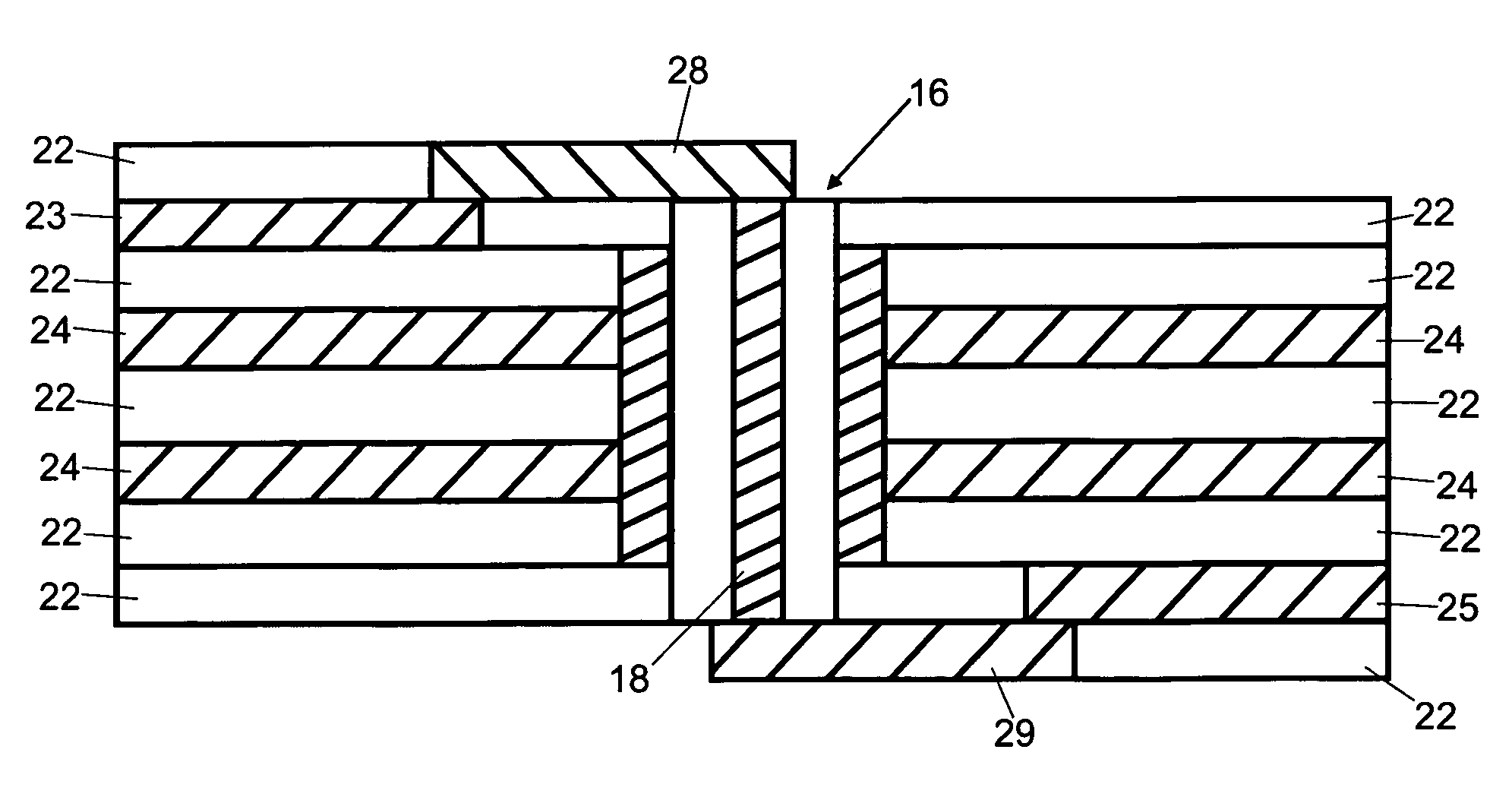
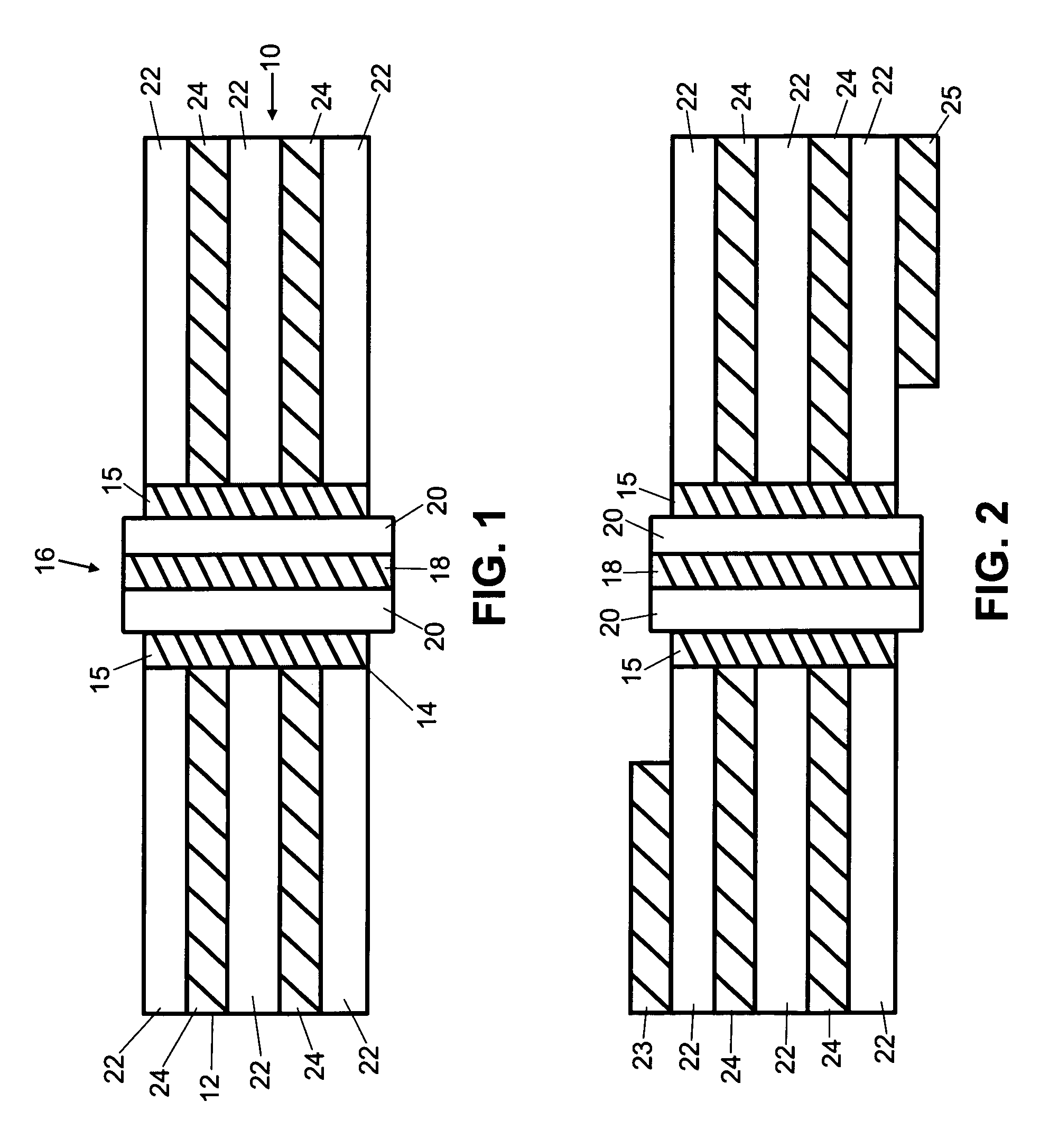
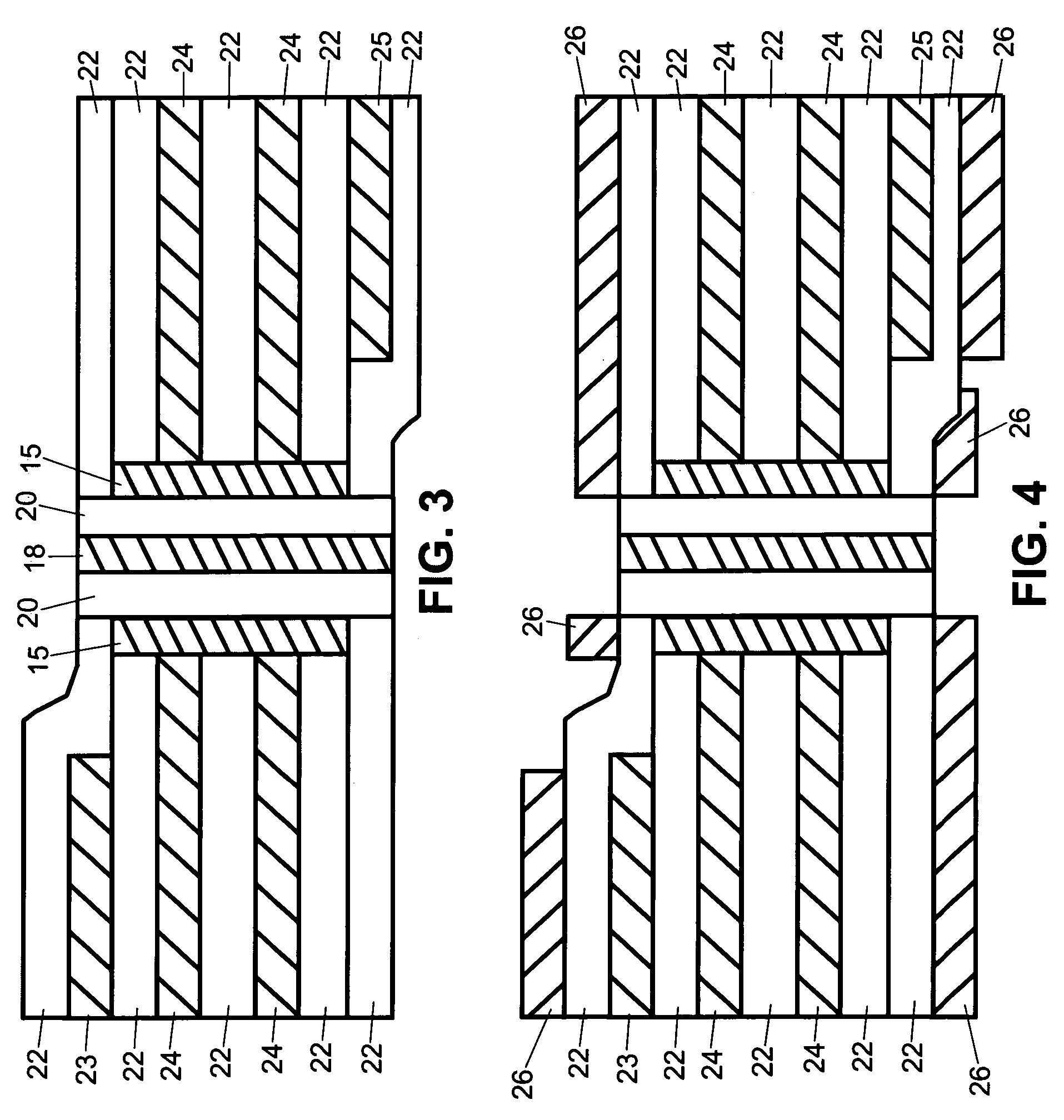
[0022]FIGS. 1-13 illustrate cutaway views of multi-layer PCBs in various stages of completion in accordance with embodiments of the present invention. Dimensions of the PCB illustrated in FIGS. 1-13 in some cases have been exaggerated for clarity. Directing attention to FIG. 1, there is shown PCB 10, having a plurality of layers 12 arranged in a stack and having formed thereon an aperture that provides via 14. As illustrated, PCB 10 includes dielectric layers 22 and ground layers 24, but power layers can also be substituted for at least some of ground layers 24 in alternative embodiments. In an embodiment, via 14 has applied to its surface within the aperture a conductive coating material 15. Conductive coating material 15 serves as the ground return of the coaxial via. It also connects all of the GND layers 24 within PCB 10. Coaxial via 16 is inserted within via 14. Coaxial via 16 is illustrated with conductive member 18 surrounded by insulating layer 20. In FIG. 2, signal layers 2...


PUM

PropertyMeasurementUnit
conductiveaaaaaaaaaa
dielectricaaaaaaaaaa
thicknessesaaaaaaaaaa

Abstract

A method of fabricating a printed circuit board having a coaxial via, includes. The method includes assembling a plurality of layers configured in a stack so that the plurality of layers has a top signal layer and a bottom signal layer; forming a hollow via through the plurality of layers to connect GND layers in the printed circuit board, forming or inserting into the hollow via a conductor coated with non-conductive material, covering the top layer and bottom layer with dielectric and patterned signal layers, covering the top layer and bottom layer with a masking agent, plating the top layer and bottom layer with a conductive material that connects signal traces within via, and removing the masking agent from the top layer and bottom layer.

Description

FIELD[0001]The present invention relates broadly to PCB assembly, and, more specifically, to configuring a coaxial via through stacked layers of a PCB.BACKGROUND OF THE INVENTION[0002]Printed circuit boards (PCBs) are typically constructed from two or more layers sandwiched together but separated by dielectric material. Layers can have different thicknesses and different dielectric material can be used within a PCB. Routing or other kinds of copper structures can be implemented at all layers. The outermost layers (top and bottom) of the PCB can have components mounted on their outside surfaces. Multilayer PCBs provide an important advantage over single layer structures in that a multilayer PCB has more routing space in a smaller footprint, which is useful for today's design imperative of smaller-size components.[0003]Vias interconnect traces on different PCB layers and connect layers to power and / or ground planes. The physical properties of a via are dictated by board geometry and a...

Claims


Application Information

Patent Timeline
Patent Type & Authority Patents(United States)
IPC IPC(8): H01K3/10
CPCH05K1/0222H05K1/115H05K3/429H05K3/4614H05K2201/09309Y10T29/49126H05K2203/061Y10T29/49165Y10T29/49162Y10T29/49128H05K2201/09809
Inventor CHENG, WHELINGKARAM, ROGERCAMERLO, SERGIO
Owner CISCO TECH INC
Why Eureka
Try Eureka