
Method for analyzing fail bit maps of waters and apparatus therefor

a failure analysis and fail bit technology, applied in electrical equipment, semiconductor/solid-state device testing/measurement, reliability increasing modifications, etc., can solve problems such as reducing lsi yields and failures that are obvious

Inactive Publication Date: 2008-07-29
KK TOSHIBA
View PDF9 Cites 13 Cited by
  • Summary
  • Abstract
  • Description
  • Claims
  • Application Information

AI Technical Summary

Benefits of technology

[0015]A still another aspect of the prevent invention inheres in a computer program product for failure analysis including program instructions for: inputting the positions of failures in a plurality of wafers; preparing a plurality of sections in the plurality of wafers; calculating for each of the sections, feature amounts that are represented by at least one numerical value representing the distribution of ...

Problems solved by technology

As LSI miniaturization progresses, various failures that reduce the LSI yields have become obvious.
The clustering distribution is a significant cause of reduction in the LSI yields.
Failures due to a manufacturing process or a manufacturing device develop manufacturing process- or manufacturing device-specific wafer failure distribution.

Method used


Image

  • Method for analyzing fail bit maps of waters and apparatus therefor
  • Method for analyzing fail bit maps of waters and apparatus therefor
  • Method for analyzing fail bit maps of waters and apparatus therefor

Examples


example 1

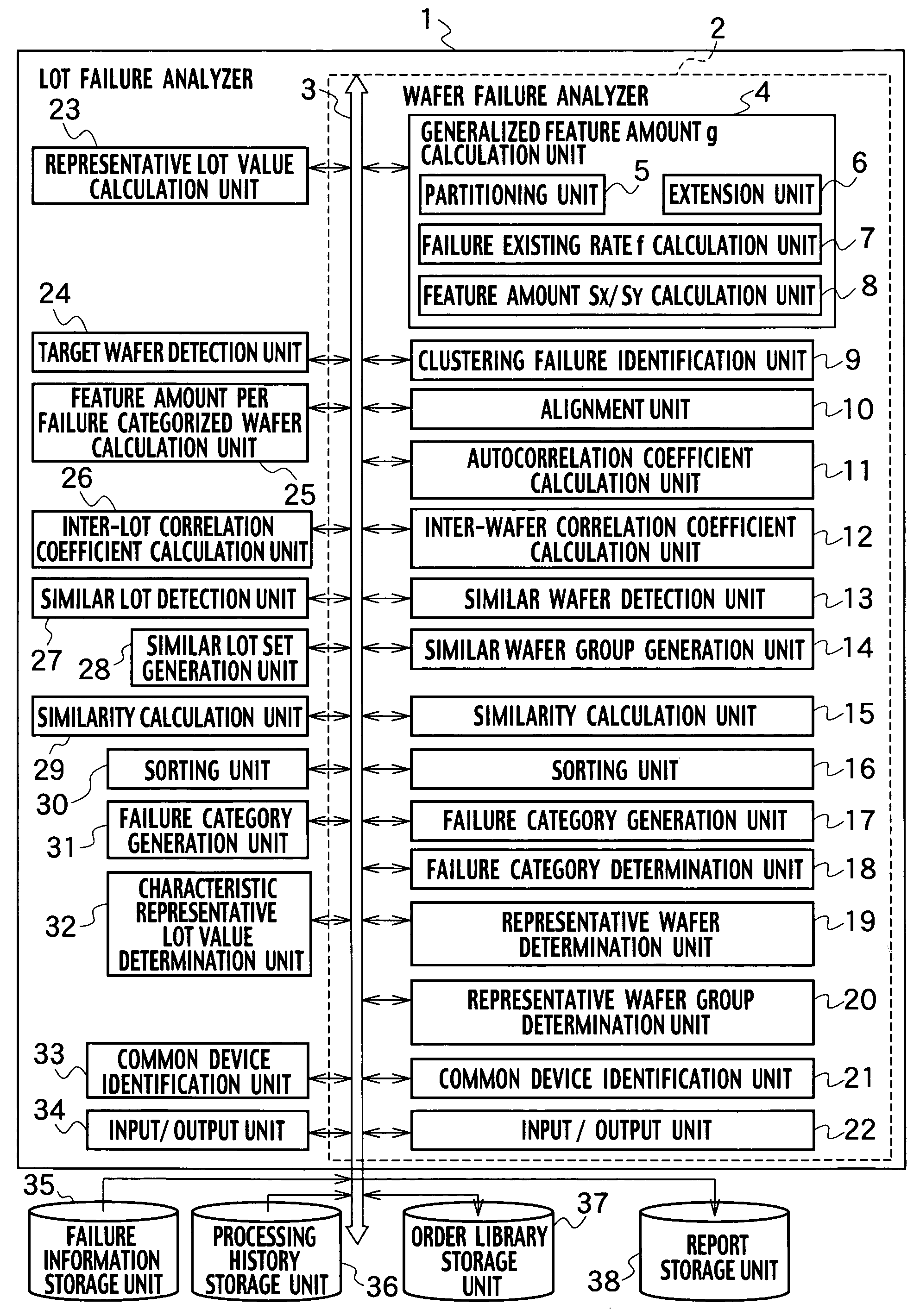
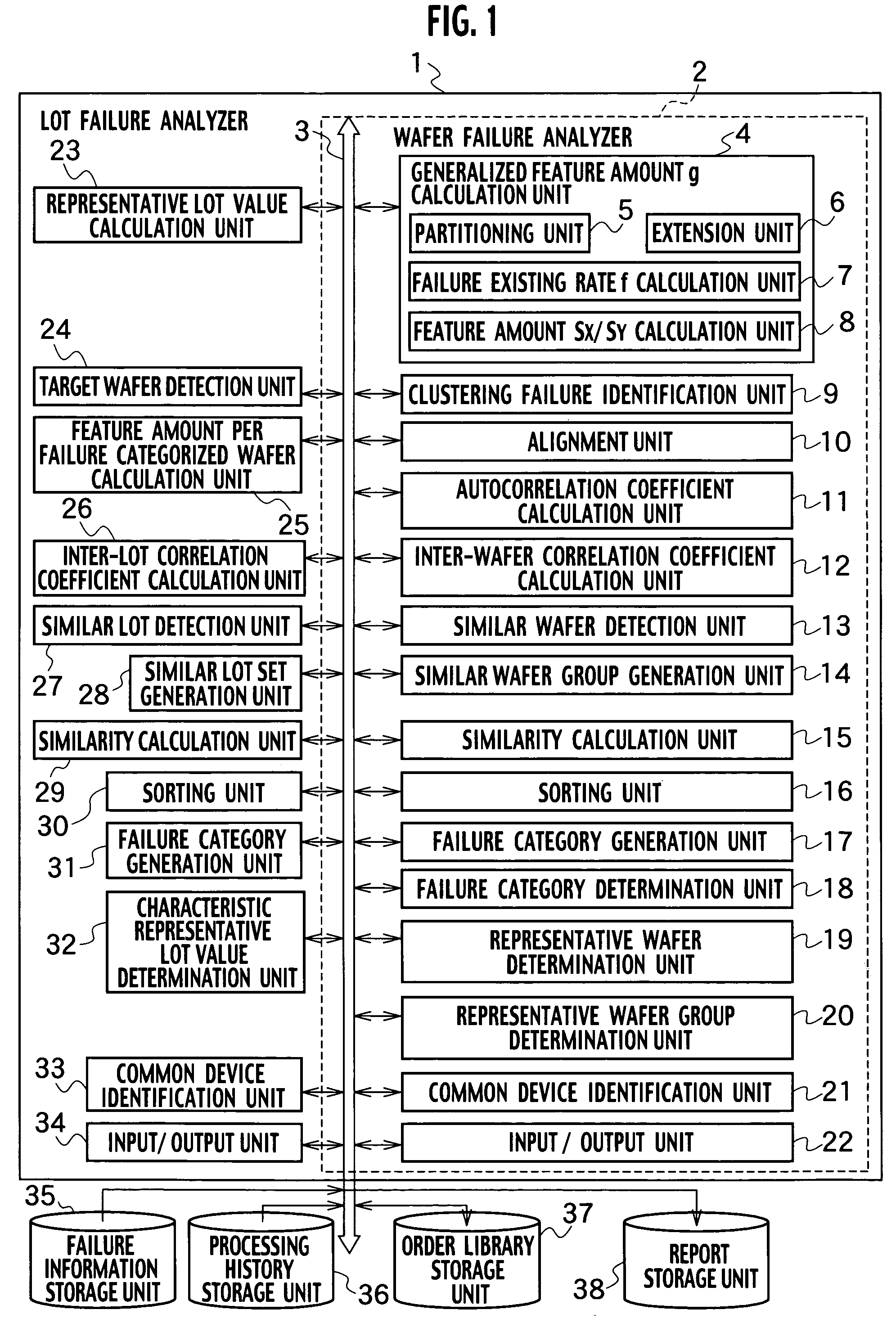
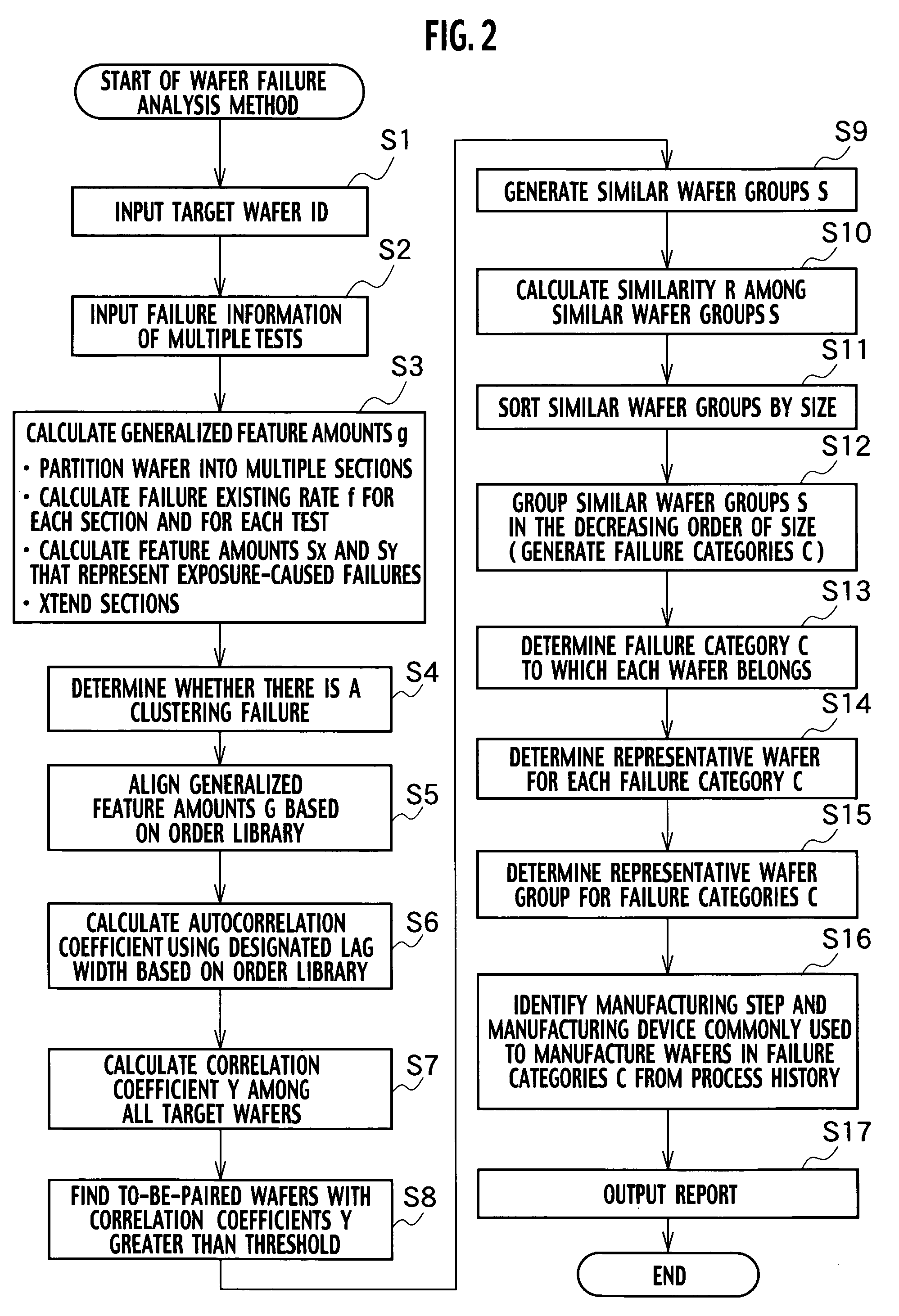
[0111]In Example 1, the wafer failure analyzer 2 in FIG. 1 and the wafer failure analysis method in FIG. 2 are described. In Example 1, wafer failure distribution is represented by a lot of numerical value groups, and wafers with similar failure distributions are automatically identified.

[0112]In step S1, a target wafer ID is input to the input / output unit 22.

[0113]In step S2, failure information as shown in FIGS. 4 through 7 is input from the failure information storage unit 35. The failure information includes wafer failure position data, which is identified within a wafer indication region 41 and a failure indication region 42. This failure information is formed based on the FBM of the failure bits in certain semiconductor memory products, which have been tested after completion of a wafer manufacturing process, and stored in the failure information storage unit 35. The wafer indication region 41 shows an existing wafer region. The failure indication region 42 shows failure bit p...

example 2

[0153]In Example 2, the failure categories C, which are sets of wafers, each having similar failure distributions, are generated from all of the wafers manufactured at a plant within a certain period such as one day or one week. Example 2 also employs the wafer failure analyzer 2 in FIG. 1 and conforms to the flowchart of FIG. 2.

[0154]To begin with, in step S1, a target wafer ID to be subjected to failure analysis is input. In Example 2, wafers to be manufactured at a plant within one day are subjected to failure analysis.

[0155]In the following, steps S2 through S9 are the same as those in Example 1.

[0156]In step S10, the similarity Rij between the similar wafer groups Si and Sj is calculated. The threshold for the similarity Rij is set to 0.5. It is determined that the similar wafer groups Si and Sj with a greater similarity Rij than the threshold of 0.5 are similar to each other.

[0157]For example, as shown in FIG. 20, the similarity R106 between the similar wafer groups S10 and S6...

example 3

[0169]In Example 3, the sections for calculating the generalized feature amounts g in step S3 of FIG. 2 are moved, expanded, and / or contracted. This allows improved accuracy in detection of wafers with similar failure distributions.

[0170]As shown in FIGS. 22 and 23, failure distributions in two wafers are extraordinarily similar to each other in that failures tend to gather at the outer regions of the wafers. It is thought that the cause of failures in those wafers in FIGS. 22 and 23 may be the same; therefore, it should be determined that those wafer failure distributions are similar to each other. However, from detailed examination based on step S3 in FIG. 2, it can be seen that the wafer in FIG. 22 has failures with clustering distribution gathering at the outer region of the wafer, in particular, in section C, and part of the failures exist in section D. In the wafer of FIG. 23, clustering failures grouped at the outer region of the wafer exist in sections C and E. The correlati...


PUM


Abstract

A failure analysis method according to the invention includes inputting the positions of failures in multiple wafers of an input device; preparing multiple sections in the multiple wafers; calculating feature amounts, which are represented by at least one numerical value representing a distribution of the failures in the multiple wafers, for each of the multiple sections; and representing by a first numerical value, the degree of similarity between the multiple wafers in terms of the feature amounts. Subsequently, the method includes detecting another wafer, which has the first numerical value greater than a predetermined first threshold, for each of the multiple wafers and forming a similar wafer group of multiple wafers with similar distributions of the failures.

Description

CROSS REFERENCE TO RELATED APPLICATIONS[0001]This application is based upon and claims the benefit of priority from prior Japanese Patent Applications No. P2003-76411, filed on Mar. 19, 2003; the entire contents of which are incorporated herein by reference.BACKGROUND OF THE INVENTION[0002]1. Field of the Invention[0003]The present invention relates to a failure analysis method that classifies wafer failure distributions in units of wafers and also in units of lot.[0004]2. Description of the Related Art[0005]In order to enhance LSI yields, clarification of the cause of deterioration in the yields, early identification of a problematic LSI manufacturing process, a problematic manufacturing device, or a problematic design condition, and improvement thereof are critical. As LSI miniaturization progresses, various failures that reduce the LSI yields have become obvious. Failure information including the test results of LSI wafers, in particular, memory products, which have been tested b...

Claims


Application Information

Patent Timeline
IPC IPC(8): H01L21/00H01L21/66H03K19/003
CPCH01L22/20
Inventor MATSUSHITA, HIROSHIKADOTA, KENICHIKAWABATA, KENJISHIOYAMA, YOSHIYUKI
Owner KK TOSHIBA
Learn More