Circuit and method for reducing fixed pattern noise

a fixed pattern and noise reduction technology, applied in the field of circuits and methods for reducing fixed pattern noise in cmos image sensors, can solve the problems of significant image quality degradation, difficulty in laying out high-performance cds(or adc) in one column pitch, etc., and achieve the effect of reducing fixed pattern nois

Active Publication Date: 2008-08-05
SAMSUNG ELECTRONICS CO LTD
View PDF4 Cites 45 Cited by
  • Summary
  • Abstract
  • Description
  • Claims
  • Application Information

AI Technical Summary

Benefits of technology

[0014]In exemplary embodiments, the present invention is directed to a circuit and method for reducing fixed pattern noise.

Problems solved by technology

Because the width of the CDS (or ADC) must be same to the pitch of the unit pixel, it is difficulty to lay out a high performance CDS(or ADC) in one column pitch.
This difference is manifested as a “checker pattern” in the image and can result in significant image quality degradation.

Method used


Image

  • Circuit and method for reducing fixed pattern noise
  • Circuit and method for reducing fixed pattern noise
  • Circuit and method for reducing fixed pattern noise

Examples


Embodiment Construction

[0051]Hereinafter, exemplary embodiments of the present invention will be described in detail with reference to the attached drawings. However, the exemplary embodiments of the present invention can be modified into various other forms, and the scope of the present invention must not be interpreted as being restricted to the exemplary embodiments described herein. The exemplary embodiments are provided to more completely explain the present invention to those skilled in the art. In the drawings, like reference numerals in the drawings denote the same elements.

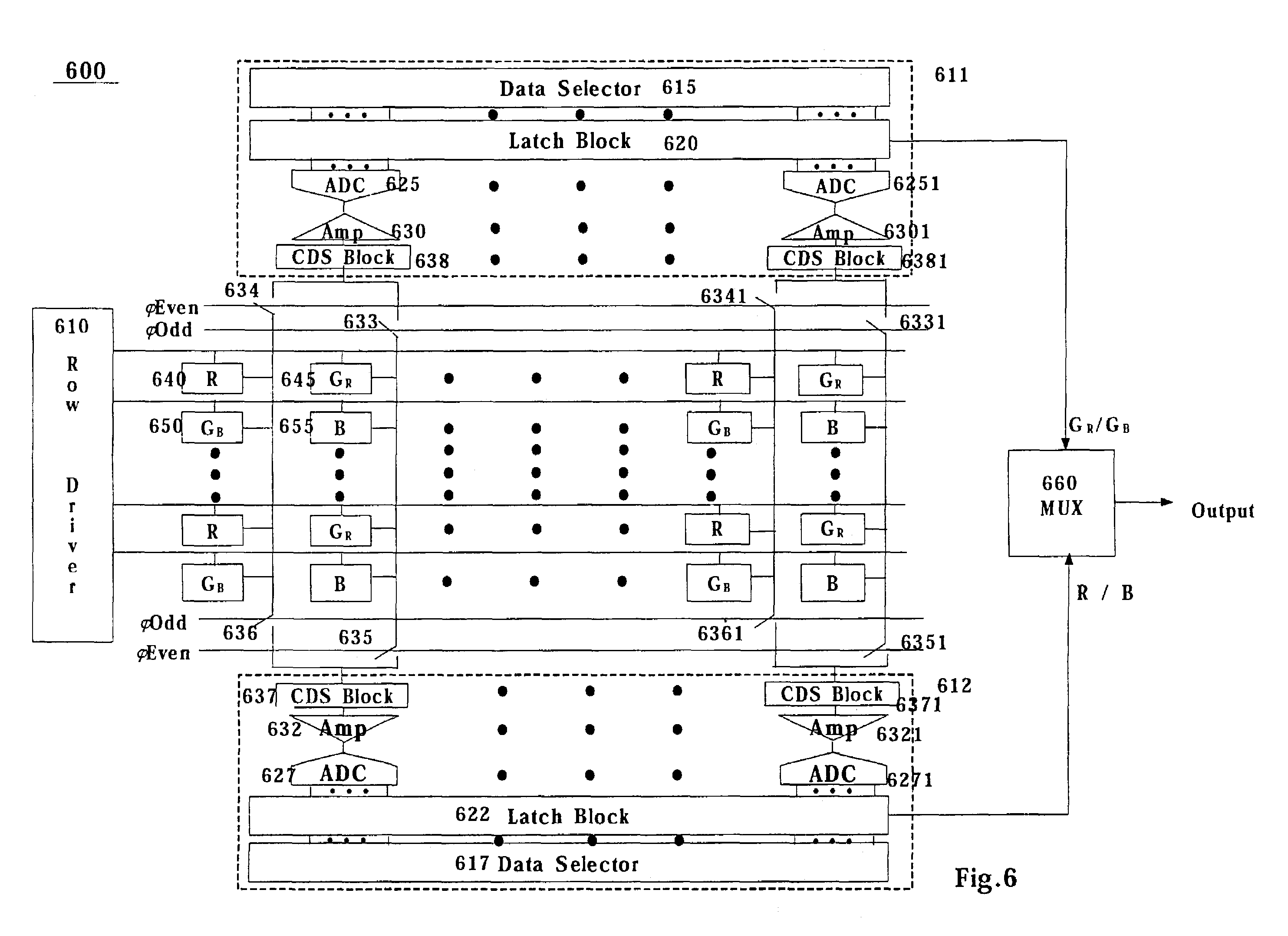
[0052]FIG. 6 shows a CMOS image sensor 600 in an exemplary embodiment of the present invention. The color pixel array has three types of pixels, red 640, blue 655 and green 645, 650. GR 645 is a green pixel located in the same row as a red pixel 640, and GB 650 is a green pixel located in same row as a blue pixel 655. Row driver 610 selects a row line in series, for example from top to bottom in response to a signal generated b...


PUM


Abstract

An image sensor and method, which includes a switching device for establishing a connection between at least one column line and one of at least two analog-to-digital converter blocks, where at least one of the at least two analog-to-digital converter blocks is connectable to at least two rows of a plurality of unit pixels. An image sensor and method, where, if a row line is odd, column outputs from odd column lines of an active pixel sensor array are connected to a first correlated double sampling block and column outputs from even column lines of the active pixel sensor array are connected to a second correlated double sampling block and if the row line is even, column outputs from odd column lines of the active pixel sensor array are connected to the second correlated double sampling block and column outputs from even column lines of the active pixel sensor array are connected to the first correlated double sampling block. An image sensor and method where a first subset of a plurality of unit pixels are connected to a first correlated double sampling block and a second subset of the plurality of unit pixels are connected to a second correlated double sampling block, where the first subset of the plurality of unit pixels are blue and red pixels and the second subset of the plurality of unit pixels are green pixels. A circuit and method for reducing fixed pattern noise.

Description

BACKGROUND OF THE INVENTION[0001]1. Field of the Invention[0002]The present invention generally relates to a circuit and method for reducing fixed pattern noise. In particular, the present invention relates to a circuit and method for reducing fixed pattern noise in a CMOS image sensor.[0003]2. Description of the Related Art[0004]FIG. 1 illustrates a conventional CMOS image sensor 100 using a Bayer-type color filter array as shown in U.S. Pat. No. 3,971,065. A color pixel array using the Bayer type color filter array has three types of pixels, red 120, blue 150 and green 130, 140. GR 130 is a green pixel located in the same row as a red pixel 120, and GB 140 is a green pixel located in same row as a blue pixel 150.[0005]Each color image signal from each pixel 120, 130, 140, 150 is converted to a digital signal by an analog to digital converter (ADC) 180. An ADC 180 is connected to each column of pixels. Each column has one ADC 180.[0006]Image signals from a single row (each row incl...

Claims


Application Information

Patent Timeline
Patent Type & Authority Patents(United States)
IPC IPC(8): H04N9/083H04N5/335H01L27/146G09G3/20H04N5/365H04N5/374H04N5/378
CPCH04N9/045H04N5/3653H04N25/672H04N25/70G09G3/20
Inventor NAM, JUNG-HYUN
Owner SAMSUNG ELECTRONICS CO LTD
Why Eureka
Try Eureka