Apparatus of high dynamic-range CMOS image sensor and method thereof

a technology of image sensor and high dynamic range, which is applied in the direction of color television, television system scanning details, television system, etc., can solve the problems of low image sensor sensitivity, extra power consumption, and limited image quality

Inactive Publication Date: 2009-01-01
CHEN OSCAL T C +2
View PDF4 Cites 15 Cited by
  • Summary
  • Abstract
  • Description
  • Claims
  • Application Information

AI Technical Summary

Benefits of technology

[0008]It is therefore a primary objective of the claimed invention to provide an apparatus of high dynamic-range CMOS image sensor and method thereof that have a charge supplement unit in the pixel circuit to provide charges to the parasitic capacitor of the photodiode for the purpose of supplying charges and delaying saturation.
[0009]It is therefore another objective of the claimed invention to provide an apparatus of high dynamic-range CMOS image sensor and method thereof that utilize a feedback circuit to duly send a trigger signal to the charge supplement unit when the node voltage of photodiode descends to a predetermined value.
[0010]It is therefore a further objective of the claimed invention to provide an apparatus of high dynamic-range CMOS image sensor and method thereof that retain the reset signal for the correlated double sampling circuit to effectively reduce the fixed pattern noise.
[0011]It is therefore a further objective of the claimed invention to provide an apparatus of high dynamic-range CMOS image sensor and method thereof that utilize the feedback circuit and charge supplement unit to make the image sensor applicable in the high contrast environment without changing exposure time and make each pixel having an independent high dynamic range.
[0012]According to the claimed invention, an apparatus of high dynamic-range CMOS image sensor and method thereof utilize a pixel circuit outputting an output signal, wherein the pixel circuit has a photodiode and a plurality of transistors; and utilize a current source as a charge supplement unit to supply current into one node of the photodiode, and providing charges to the parasitic capacitor of the photodiode to delay saturation in the pixel circuit. In addition, a feedback circuit can be further designed connecting the pixel circuit. The feedback circuit has a PMOS source follower and a PMOS inverter, and after receiving the output signal from the pixel circuit, the feedback circuit will generate a control signal according to this output signal to control status of the charge supplement unit and then enhance the dynamic range of the CMOS image sensor.

Problems solved by technology

In the conventional technologies, the photonic signal compression method will lower the sensitivity of an image sensor, especially the signal noise ratio will be smaller under low illumination, and the Correlated Double Sampling (CDS) circuit cannot be used to reduce the Fixed Pattern Noise (FPN) due to no reset signal, so the image quality is limited.
In addition, this method combining linear and logarithmic integration modules will make extra power consumption and increase design complexity of the signal processing circuit.
This backend circuit will enlarge the chip size, and its processing time will reduce the reading speed that makes the sensor cannot capture images immediately.

Method used


Image

  • Apparatus of high dynamic-range CMOS image sensor and method thereof
  • Apparatus of high dynamic-range CMOS image sensor and method thereof
  • Apparatus of high dynamic-range CMOS image sensor and method thereof

Examples


Embodiment Construction

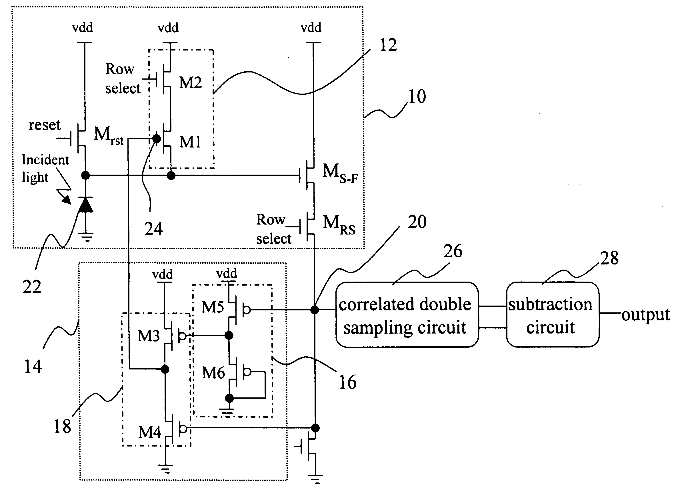
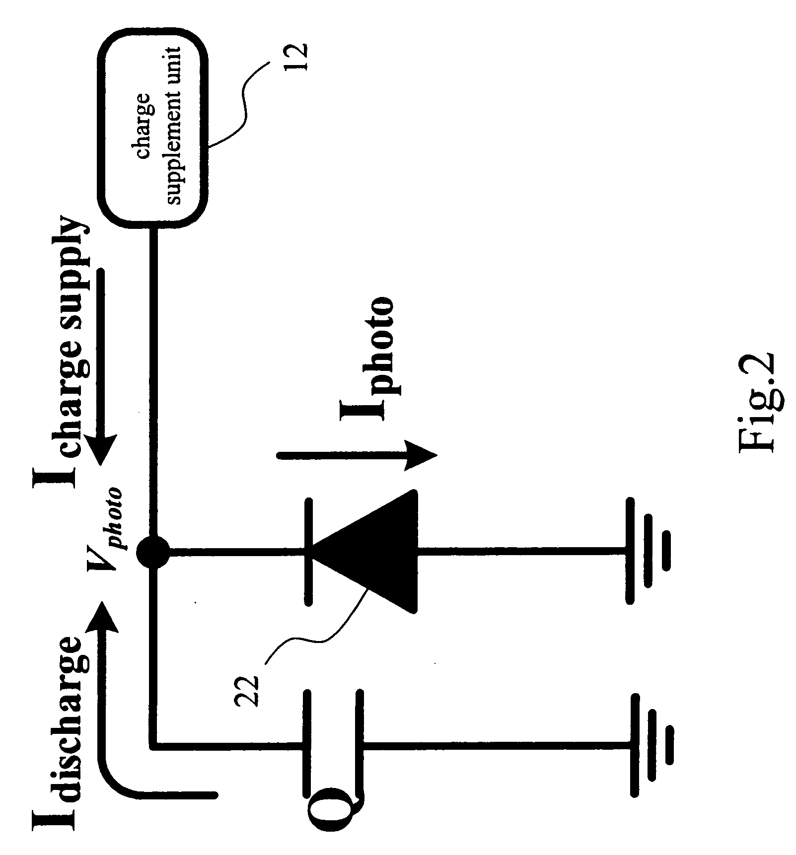
[0025]The present invention discloses an apparatus of high dynamic-range CMOS image sensor and method thereof. The present invention provides charge supplement with a charge supplement unit, and the charge supplement unit can be controlled by using an external bias voltage or connecting a feedback circuit to enable that the saturation time of the parasitic capacitor of the photodiode can be delayed and the dynamic range of the image sensor can be enlarged. The present invention also has the advantages of low noise, high sensitivity and low complexity.

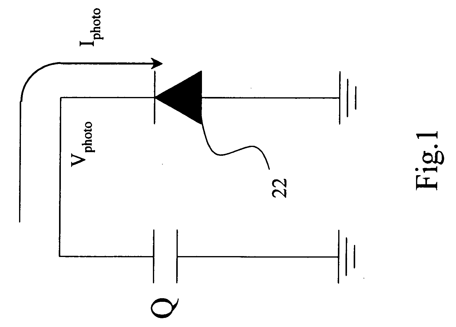
[0026]As shown in FIG. 1, after resetting the photodiode 22, the N terminal is biased to a high voltage level and this bias makes the parasitic capacitor having induced charge Q. Amount of the charge is reacted on the voltage V.sub.photo of the N terminal of the photodiode 22, wherein I.sub.photo is the photo current of the photodiode 22 after illuminated, and the charges will be discharged through the path of the photo current. When th...


PUM


Abstract

The present invention discloses an apparatus of high dynamic-range CMOS image sensor and method thereof. The present invention utilize a pixel circuit outputting an output signal, wherein the pixel circuit has a photodiode and a plurality of transistors; and utilize a current source as a charge supplement unit to supply current into one end of the photodiode, and providing charges to the parasitic capacitor of the photodiode to delay saturation in the pixel circuit. In addition, a feedback circuit can be further designed connecting the pixel circuit. The feedback circuit receives the output signal from the pixel circuit and then outputs a control signal according to the output signal of the pixel circuit to control status of the charge supplement unit, and thereby increasing the dynamic range of the CMOS image sensor.

Description

RELATED APPLICATIONS[0001]This application is a Divisional patent application of co-pending application Ser. No. 11 / 211,670, filed on 26 Aug. 2005. The entire disclosure of the prior application, Ser. No. 11 / 211,670, from which an oath or declaration is supplied, is considered a part of the disclosure of the accompanying Divisional application and is hereby incorporated by reference.BACKGROUND OF INVENTION[0002]1. Field of the Invention[0003]The invention relates to an apparatus of high dynamic-range CMOS image sensor and method thereof, and more particularly, to an apparatus of high dynamic-range CMOS image sensor and method thereof that providing charge supplement to the photodiode.[0004]2. Description of the Prior Art[0005]Dynamic range is an important norm to evaluate quality of an image sensor. Larger the dynamic range, larger the sensible range from lowest sensible signal to highest unsaturated signal of the image sensor is.[0006]Technologies of designing image sensors with hi...

Claims


Application Information

Patent Timeline
Patent Type & Authority Applications(United States)
IPC IPC(8): H04N5/335H04N5/355H04N5/3745H04N5/378
CPCH01L27/14609H04N5/374H04N5/35518H04N25/573H04N25/76
Inventor CHEN, OSCAL T.-CLIU, WEI-JENYEH, HSIU-FEN
Owner CHEN OSCAL T C
Why Eureka
Try Eureka