CMOS imager with wide dynamic range Pixel

a technology of pixel and dynamic range, applied in the field of semiconductor image sensors, can solve the problems of non-linear operation of the sensor, increased noise, and loss of dynamic range available for the integration of the photodiode, and achieve the effect of improving performance, reducing the amount of additional circuitry, and not significantly increasing the pixel cell siz

Inactive Publication Date: 2007-02-01
IMAGERLABS
View PDF4 Cites 14 Cited by
  • Summary
  • Abstract
  • Description
  • Claims
  • Application Information

AI Technical Summary

Benefits of technology

[0017] According to one aspect of the present invention, an active pixel sensor has a wide dynamic range through automatic voltage swing recovery for the output source follower. An active pixel sensor cell array may be implemented with minimum additional circuitry and without significantly increasing the pixel cell size. In one embodiment, an active pixel sensor cell in an active pixel sensor array improves performance by simultaneously recovering dynamic range losses, providing signal gain in the pixel, reducing fixed pattern noise (FPN), improving array uniformity, and eliminating previous signal noise known as “ghost image”.

Problems solved by technology

The voltage drifts with temperature changes, and thus the amount of loss in the dynamic range available for the photodiode integration drifts as well.
This results in non-linear operation of the sensor, especially at low signal levels, and increased noise.
In addition, pixel 100 suffers from increased noise and non-linearity due to un-cleared output voltage of previous integration prior to transferring voltage representing the newly integrated charge (also referred to as “image ghost”).
Furthermore, the pixel 100 suffers from decreased dynamic range due to clipping of the signal high range or the signal low range depending on the polarity of the photo-diode and the circuitry.

Method used


Image

  • CMOS imager with wide dynamic range Pixel
  • CMOS imager with wide dynamic range Pixel
  • CMOS imager with wide dynamic range Pixel

Examples


Embodiment Construction

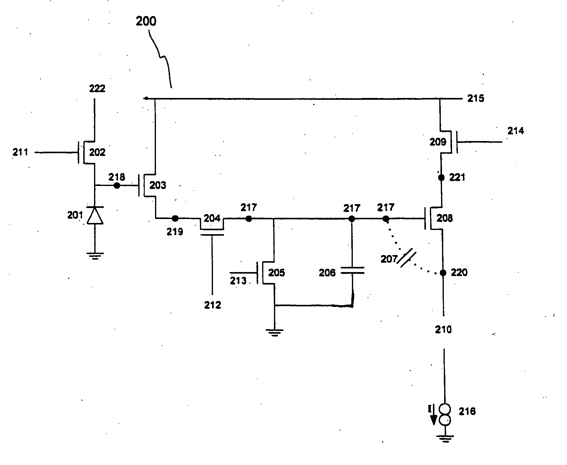
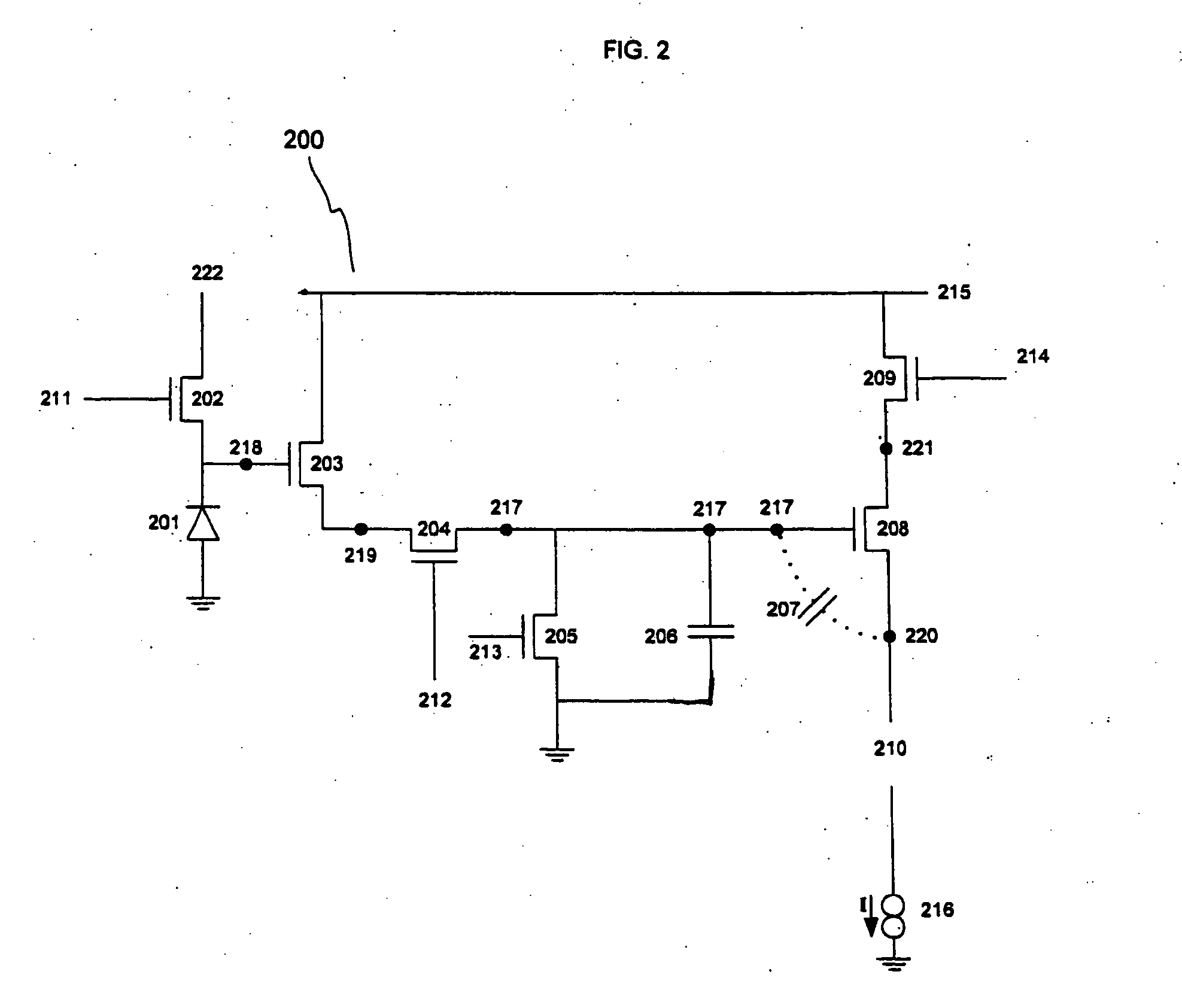
[0029]FIG. 2 is a schematic diagram of a portion of a CMOS active pixel sensor array that comprises an active pixel sensor cell 200 in accordance with one embodiment of the current invention. The cell 200 may be connected to additional cells contained in the array via a column output bus 210 having a current source 216 coupled to ground. The cell (or “pixel”) 200 comprises a light sensing device 201 that is not limited to, but in this case is, a reversed bias photodiode overlying a doped region of a substrate for accumulating photon-generated charge during the integration period.

[0030] The pixel 200 further contains a reset switch transistor 202 that is controlled by a reset clock 211 for resetting the photodiode 201 to a predefined voltage prior to integration. The drain of the reset transistor 202 is connected to a reset voltage supply (RST) 222, and upon application of the reset clock signal 211, it resets the photodiode high to the positive voltage RST minus the threshold of th...


PUM


Abstract

In one aspect of the present invention, a light sensor is provided in the active pixel sensor cell for sensing incident radiation. The voltage corresponding to the photon-generated or other radiation-generated charge in the active pixel sensor cell is stored on a storage node via a sample-and-hold capacitor. Additional elements, such as source-follower transistors, may reside between the sensing element and the sample-and-hold capacitor. The signal is read via a readout source-follower (RSF) transistor. The readout source-follower drain is connected to the row select switch while its drain is connected to the output node on the column output bus. This configuration couples the storage node to the gate-source capacitance of the readout source-follower transistor. This allows the voltage on the storage node to increase proportionally to the increase in voltage on the readout node when the row select is closed and thus enables the drain current to flow through the RSF to the column output bus.

Description

RELATED APPLICATION [0001] The present application is based on and claims priority to U.S. Provisional application Ser. No. 60 / 703,199, filed Jul. 28, 2005.BACKGROUND [0002] 1. Field of the Invention [0003] The present invention relates to the field of semiconductor devices and, in particular, to complementary metal oxide semiconductor (CMOS) image sensors. [0004] 2. Related Art [0005] Thanks to the latest advances in technology, CMOS imagers have been used in various applications and have not been limited any more to consumer low-end applications only. [0006] A typical CMOS imager comprises of a focal plane array of pixel cells, each one of the pixels further comprising a light detection component such as a photodiode, a photogate or a photoconductor. The pixel also has a readout circuit that is connected to its light detection node and may also include a sample-and-hold circuit for electronic shutter control either before or after the readout circuit. The CMOS imager pixel cell ma...

Claims


Application Information

Patent Timeline
Patent Type & Authority Applications(United States)
IPC IPC(8): H01L29/768
CPCH01L27/14609H04N5/37452H04N5/3597H04N5/3559H04N25/59H04N25/626H04N25/771
Inventor JOHNSON, KIM LORENATLAS, EUGENENETER, SARIT
Owner IMAGERLABS
Why Eureka
Try Eureka