Semiconductor memory device and method of adjusting same

a memory device and semiconductor technology, applied in the field of semiconductor memory devices, can solve the problems of limiting system processing speed, difficult to restrict the tis/tih of all products within, and failure to generate command signals under strict tis/tih conditions at high operating frequency

Inactive Publication Date: 2008-08-12
PS4 LUXCO SARL
View PDF5 Cites 37 Cited by
  • Summary
  • Abstract
  • Description
  • Claims
  • Application Information

AI Technical Summary

Benefits of technology

[0034]It is therefore an object of the present invention to provide a semiconductor memory device which is capable of always retrieving data written into anti-fuses, and which is capable of adjusting the timing of an internal signal when an initial setting is made, and to provide a method of adjusting the same.
[0037]Also, even in future semiconductor memory devices which are expected to operate at increasingly higher clock frequencies, since the Fuse data written into the anti-fuses is always delivered. Therefore, it is possible to obtain a semiconductor memory device that meets a specified value of tIS / tIH of the internal signal to the clock. Consequently, the manufacturing yield rate of semiconductor memory devices is improved.

Problems solved by technology

Recent information processing apparatuses and the like are bottlenecked on access speeds to semiconductor memory devices, which limit system processing speeds, as a result of an increase in processing speeds performed by CPU.
However, it is difficult to restrict tIS / tIH of all products within the specified range of values mentioned above when taking into account variations in manufacturing.
However, these signals are indefinite and therefore may sometimes cause a failure during the initial settings.
Also, in a configuration where command signals are internally generated for initial settings, a shift in tIS / tIH of CLK and CMD, if any, can cause a failure to generate a command signal under strict tIS / tIH conditions at high operating frequencies.
Stated conversely, a command signal can be always generated by adjusting the timing, but before the adjustment, there is no guarantee that the command signal will always be generated because how the delay amount of internal signal will be set when an initial setting is made is not known.
Accordingly, future semiconductor memory devices, which are required to operate at higher frequencies, will encounter difficulties in ensuring secure operations because of these indefinite factors.
For this reason, if clock CLK and CMDB signal shift in phase relationship when an initial setting is made as shown in FIG. 6, this shift can cause tIS / tIH to fall out of the specified range of values, resulting in a failure to generate the PMDCMDT signal from the latch circuit and a consequent failure to generate the Fuse read signal.
In this event, since Fuse data are not delivered from the anti-fuse block, the delay amount of the CMDB signal is not switched in the delay amount switching circuit, thus impeding normal operation of the semiconductor device.
Also, a failure to generate Fuse read signal would disable an adjustment test for writing Fuse data into anti-fuses (the aforementioned adjustment of the timing for an internal signal), which is performed after assembly of the semiconductor memory device.
In future semiconductor memory devices, in particular, which are expected to operate at increasingly higher clock frequencies, increasingly more strict restrictions will be imposed on the aforementioned tIS / tIH, thus making it more difficult to guarantee normal operation of the semiconductor memory device due to the indefinite factors as mentioned above.

Method used


Image

  • Semiconductor memory device and method of adjusting same
  • Semiconductor memory device and method of adjusting same
  • Semiconductor memory device and method of adjusting same

Examples


Embodiment Construction

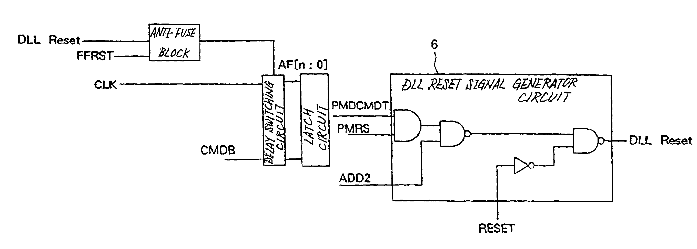
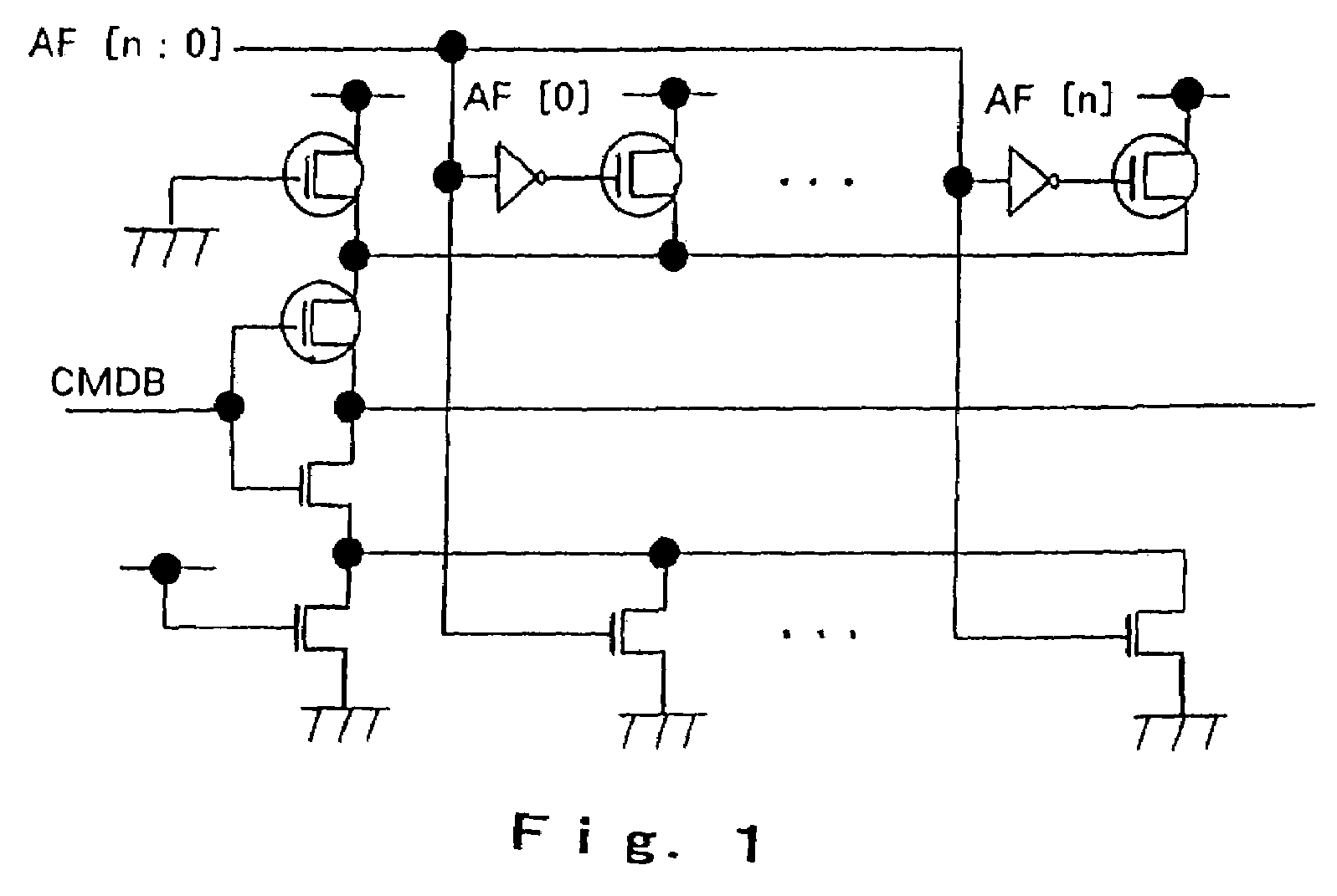
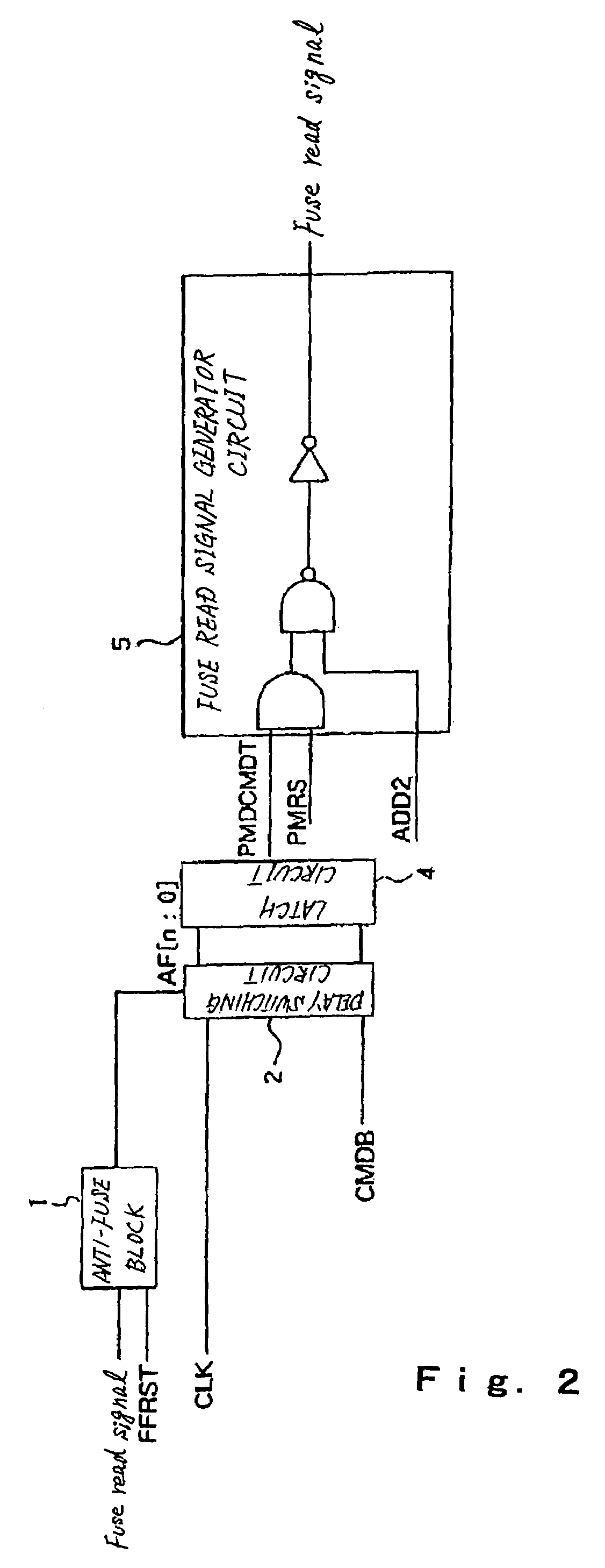
[0048]As illustrated in FIG. 7, an anti-fuse control circuit according to the present invention differs from the conventional anti-fuse control circuit illustrated in FIG. 1 in that a DLL reset signal generator circuit is substituted for Fuse read signal generator circuit 5. Since the remaining configuration and operation of the present invention are basically similar to the conventional anti-fuse control circuit, a description thereon is omitted.

[0049]As illustrated in FIG. 7, DLL reset signal generator circuit 6 included in the anti-fuse control circuit according to the present invention generates a DLL Reset signal based on a PMDCMDT signal supplied from a latch circuit, in a manner similar to conventional read signal generator circuit 5. In this event, DLL reset signal generator circuit 6 receives instructions, in accordance with the values of a PMRS signal and an ADD2 signal which are code signals, whether or not to deliver the DLL Reset signal.

[0050]Further, DLL reset signal g...


PUM


Abstract

A DLL Reset signal for delivering Fuse data from anti-fuses is generated from a reset signal which is supplied asynchronous to a clock when an initial setting is made. The DLL Reset signal is supplied to an anti-fuse block which comprises a plurality of anti-fuses, such that the delay amount of an internal signal is switched to a desired value in accordance with the Fuse data written into the anti-fuses.

Description

BACKGROUND OF THE INVENTION[0001]This application is based upon and claims the benefit of priority from Japanese Patent Application No. 2005-313387 filed on Oct. 27, 2005, the content of which is incorporated by reference.[0002]1. Field of the Invention[0003]The present invention relates to a semiconductor memory device which is configured to adjust the delay amount of an internal signal using data written into anti-fuses.[0004]2. Description of the Related Art[0005]Recent information processing apparatuses and the like are bottlenecked on access speeds to semiconductor memory devices, which limit system processing speeds, as a result of an increase in processing speeds performed by CPU. Thus, there is demand for a reduction in the time required to write and read data into and from semiconductor memory devices, and has been addressed by using DRAM (Dynamic Random Access Memory), SDRAM (Synchronous DRAM) and the like which operate at clock speeds at several hundred MHz. Further, deve...

Claims


Application Information

Patent Timeline
Patent Type & Authority Patents(United States)
IPC IPC(8): G11C17/18
CPCG11C7/22G11C17/18G11C17/16G11C7/222
Inventor NISHIOKA, NAOHISAFUJISAWA, HIROKI
Owner PS4 LUXCO SARL
Why Eureka
Try Eureka