Film forming method for manufacturing planar periodic structure having predetermined periodicity

a film forming and periodic structure technology, applied in the direction of conductive pattern formation, semiconductor/solid-state device details, instruments, etc., can solve the problems of high cost, long manufacturing time, and uneven light transmissivity to the plane of the color filter, so as to reduce the irregularity of film formation

Active Publication Date: 2008-08-19
KATEEVA
View PDF8 Cites 11 Cited by
  • Summary
  • Abstract
  • Description
  • Claims
  • Application Information

AI Technical Summary

Benefits of technology

[0018]In the first case (A-1) the first liquid material U1 is deposited at the center of region P, so that following liquid drop Q2 is integrated with the liquid material U1 already deposited at the center of the region P even if the following liquid drop Q2 is supplied to a position diverted from the center of region P. Therefore, a liquid material U2 relating to liquid drops Q1, Q2 is also arranged almost at the center of region P as illustrated in A-2. At this time, as shown in A-3 and A-4, even if liquid drops Q3, Q4 are supplied in sequence, liquid materials U3, U4 can be easily and uniformly deposited. If the liquid material is equally deposited within region P, a liquid material U4 is dried at last to result in an almost equally formed film as indicated with a long dot line in A-4.
[0056]Still further, the present invention provides a display device formed using the method for manufacturing a display device described above. According to this method, it is possible to construct a display device with high display quality by reducing the irregularity in film formation caused by the film-forming process. Particularly, in pixel rows arranged in the scanning direction, a greater improvement is made in the present invention than in the prior art because there is a smaller deviation in the film structure between pixels. As a result, it is possible to produce a display device with a reduction in the irregular color or brightness irregularity but with a remarkable increase in optical uniformity as compared with the prior art.

Problems solved by technology

However, the patterning process using photolithography requires several complicated, time-consuming processes such as coating, exposure and development of materials, and a large quantity of respective color materials or resists are consumed which leads to a problem of high costs.
As a result, there is a problem that the light transmissivity to a plane of a color filter is not uniform.
However, if a scanning process is performed in the aforementioned way, the number of scanning processes is rapidly increasing which makes the manufacturing time longer, thereby resulting in a problem of lowering production efficiency.
However, the inventor found that it is impossible to eliminate a stripe pattern color irregularity in spite of the minimization of a difference in the amount of ink among respective filter elements in the aforementioned method if the color filter is manufactured in the conventional apparatus.
In other words, the deviated state of ink charged in the respective filter elements results in a difference in the amount of transmissive light depending upon places, which makes a stripe pattern of color irregularity noticeable.
Further, as shown in B-3 and B-4 of FIG. 30, the liquid materials U3″ and U4″ flooded out of region P result in a cause of mixed colors and an increase of irregularity in case of a color filter or an EL device for example.
At this time, it becomes difficult to stop unequal deposition of the liquid material in the region P even though the liquid drop is additionally supplied.
However, in actuality, if the driving period Td of the liquid drop supplying means is small, the supply of the liquid material is not sufficient for the liquid drop supplying means.
Therefore, there is a limitation to an increase in the driving frequency of the liquid drop supplying means.
Accordingly, if the driving period Td is small, a deviation in the supplying positions of the liquid drop among regions P decreases to restrict irregularity in film formation, but there are problems that productivity decreases and that film-forming defects increase.
On the contrary, if resolution Rx is small, the difference in the supplying position of the liquid drop among regions P as seen from the scanning direction X is small, but the manufacturing efficiency decreases and resultant defects easily occur because the supplying amount of the liquid material as the liquid drop decreases.

Method used


Image

  • Film forming method for manufacturing planar periodic structure having predetermined periodicity
  • Film forming method for manufacturing planar periodic structure having predetermined periodicity
  • Film forming method for manufacturing planar periodic structure having predetermined periodicity

Examples


embodiment

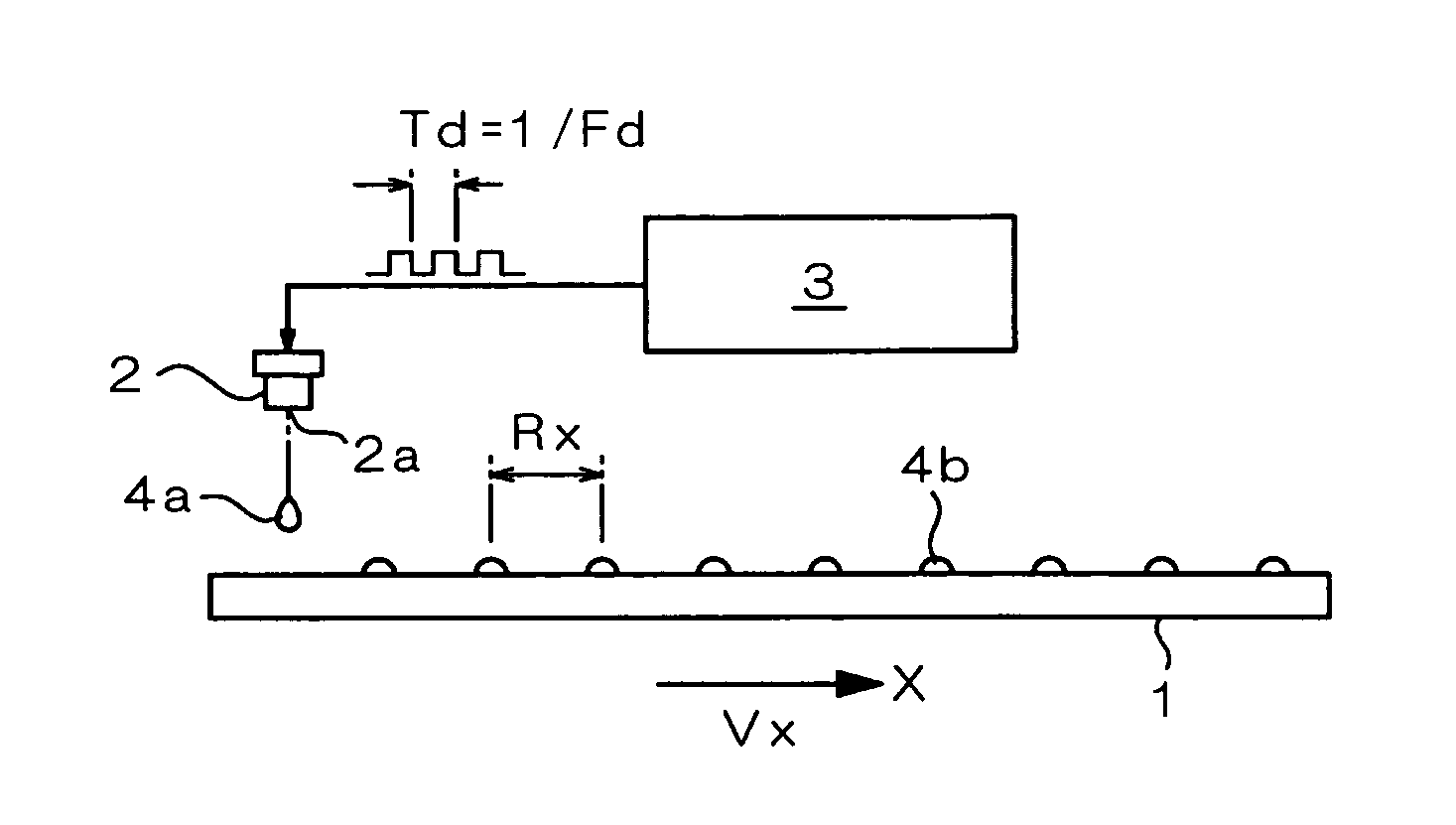
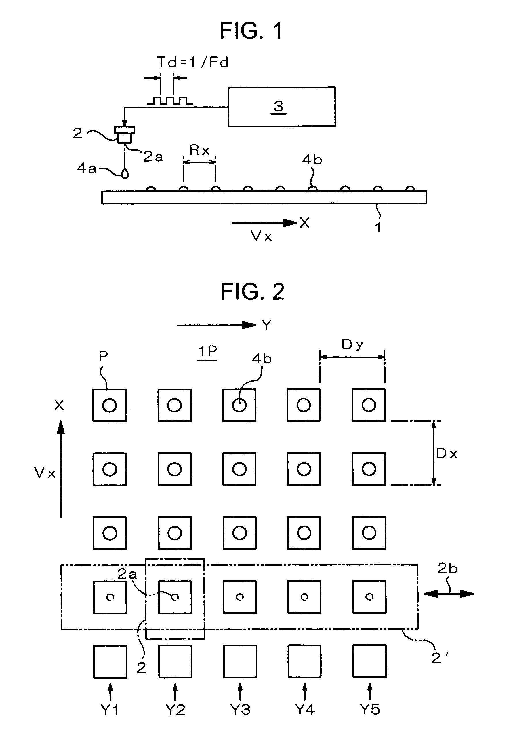
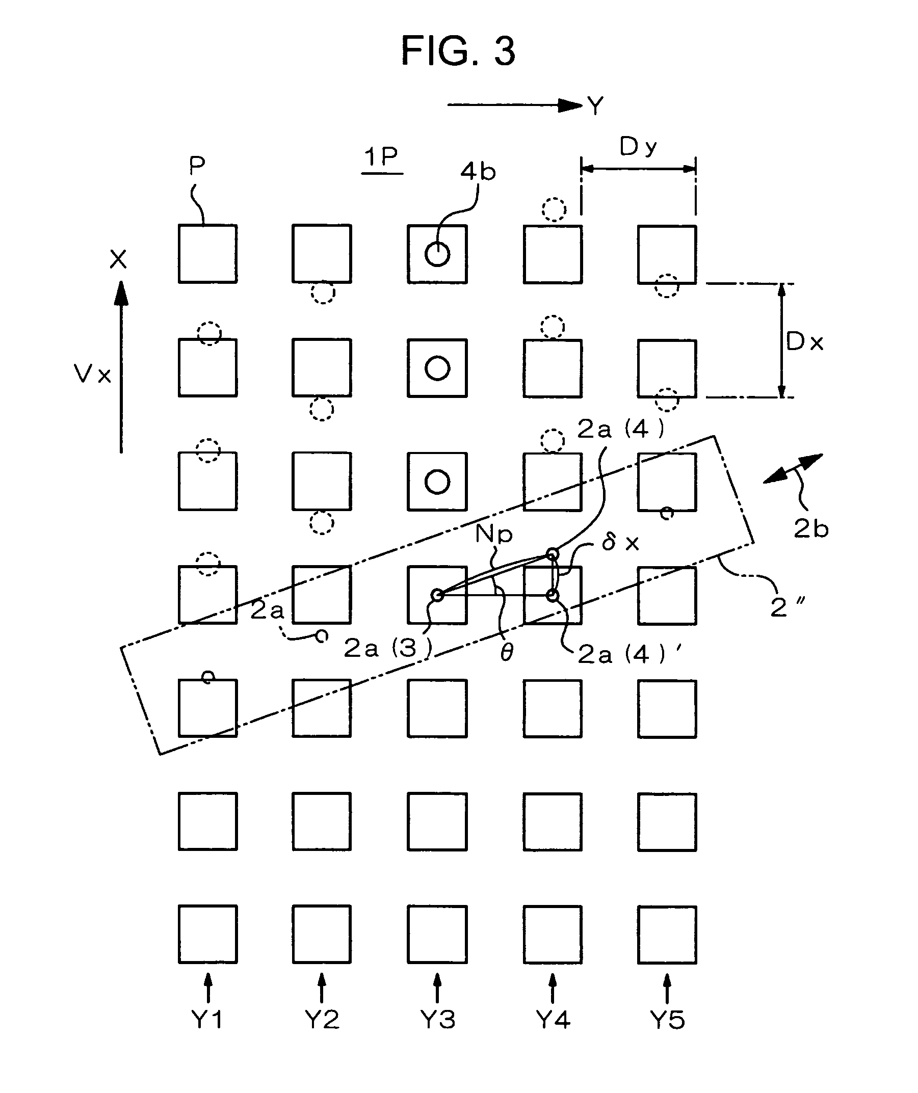
[0156]Next, more specific embodiments corresponding to the aforementioned description will be described below. FIG. 7 illustrates a planar periodic pattern (color pattern) 1P′ referred to as a delta arrangement. A specific embodiment of the planar periodic pattern 1P′ may include an arrangement pattern of filter elements of a color filter or an arrangement pattern in a light emitting area of an EL device, which will be described below. One of a plurality of types of color elements R, G, B is formed in a plurality of regions P arranged in the planar periodic pattern 1P′. In this case, a structural period as seen from the scanning direction X in the planar periodic pattern 1P′ is classified into a small structural period dx, when the regions P of all the color elements R, G, B are regarded as an identical structural unit, and into a large structural period Dx when the color elements R, G, B are respectively regarded as a different structural unit. Similarly to this, a structural perio...


PUM

PropertyMeasurementUnit
diameteraaaaaaaaaa
diameteraaaaaaaaaa
angle of inclinationaaaaaaaaaa

Abstract

A film-forming method is provided for forming a planar periodic structure having a predetermined periodicity by depositing liquid material on an object. A liquid drop supplying means is used which supplies a liquid drop at a predetermined driving period to deposit the liquid material on the object; the presence or absence of the supply of the liquid drop is controlled at each driving period in accordance with the periodicity of the planar periodic structure to be formed; and the liquid drop is supplied by controlling the liquid drop supplying means while the liquid drop supplying means is scanned at a predetermined scanning speed in a predetermined scanning direction relative to the object. A natural number times a value obtained by multiplying the driving period and the scanning speed is set to be the structural period of the planar periodic structure in the scanning direction.

Description

RELATED APPLICATIONS[0001]This application claims priority to Japanese Patent Application No. 2003-060253 filed Mar. 6, 2003 which is hereby expressly incorporated by reference herein in its entirety.BACKGROUND OF THE INVENTION[0002]1. Technical Field of the Invention[0003]The present invention relates to a film-forming method, a film-forming apparatus, an apparatus and a method for manufacturing a color filter substrate, an apparatus and a method for manufacturing a substrate for an electroluminescent device, a method for manufacturing a display device, a display device, and an electronic apparatus. More specifically, the present invention relates to a manufacturing technique for forming a film by supplying liquid material in a liquid drop state.[0004]2. Description of the Related Art[0005]In general, there are known a variety of display devices using as a display means an electro-optical apparatus such as a liquid crystal display device or an electroluminescent device (hereinafter...

Claims


Application Information

Patent Timeline
Patent Type & Authority Patents(United States)
IPC IPC(8): B05D5/06B41J2/01B05D1/26B05D7/00G02B5/20G02F1/13G02F1/1335H01B13/00H01J11/20H01J11/42H01J11/44H01L21/288H01L21/3205H01L21/768H01L23/522H01L51/00H01L51/40H01L51/50H05B33/10H05B33/26H05K3/10
CPCH01L51/0005H10K71/135H05B33/10
Inventor ITO, TATSUYAOYAMA, TAKESHI
Owner KATEEVA
Why Eureka
Try Eureka