Bidirectional photothyristor chip, optical lighting coupler, and solid state relay

a bidirectional, optical lighting technology, applied in emergency protective devices, coupling device connections, coupling device details, etc., can solve the problems of non-direct relation, failure to suppress, and conventional bidirectional photothyristor, so as to reduce the lifetime of holes, prevent the photothyristor section, and enhance the dv/dt characteristic

Active Publication Date: 2008-09-09
SHARP KK
View PDF11 Cites 203 Cited by
  • Summary
  • Abstract
  • Description
  • Claims
  • Application Information

AI Technical Summary

Benefits of technology

[0015]An object of the present invention is to provide a bidirectional photothyristor chip capable of improving luminous sensitivity as well as a commutation characteristic and a critical rate of rise of off-state voltage dv / dt characteristic which are in a trade-off relation with the luminous sensitivity.

Problems solved by technology

However, the conventional bidirectional photothyristor has a following problem.
More particularly, the commutation characteristic and the dv / dt characteristic are in a trade-off relation with the luminous sensitivity, which are the most important design issue in terms of the performance of the bidirectional photothyristor.
There is a trade-off correlation that higher sensitivity decreases the commutation characteristic, and therefore how to increase the commutation characteristic is an issue in pursuit of higher sensitivity.
However, such structure has no direct relation with improvement of the commutation characteristic and therefore fails to suppress the holes 11 which are generated on the side of the photothyristor 2 and remain in the N-type silicon substrate 1 from moving to the P gate diffusion region 6′ on the side of the photothyristor 3.
This kind of malfunction tends to occur particularly in the high temperature condition.
More particularly, how to enhance the dv / dt characteristic is also an issue in pursuit of higher sensitivity.

Method used


Image

  • Bidirectional photothyristor chip, optical lighting coupler, and solid state relay
  • Bidirectional photothyristor chip, optical lighting coupler, and solid state relay
  • Bidirectional photothyristor chip, optical lighting coupler, and solid state relay

Examples


first embodiment

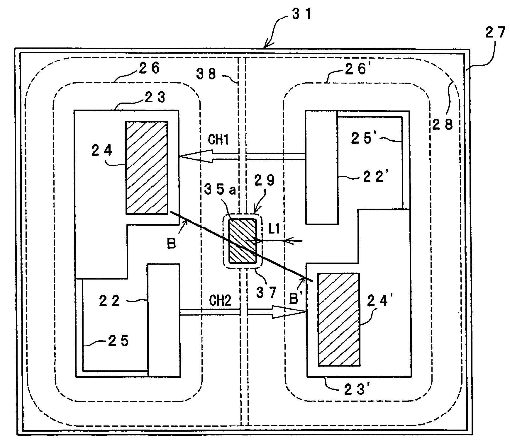
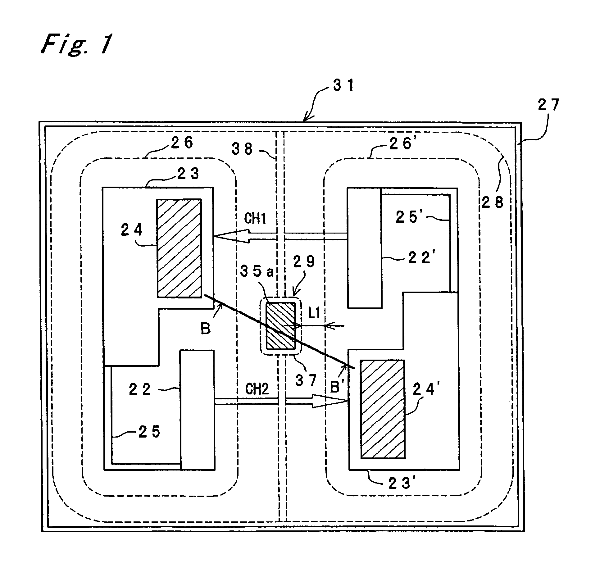
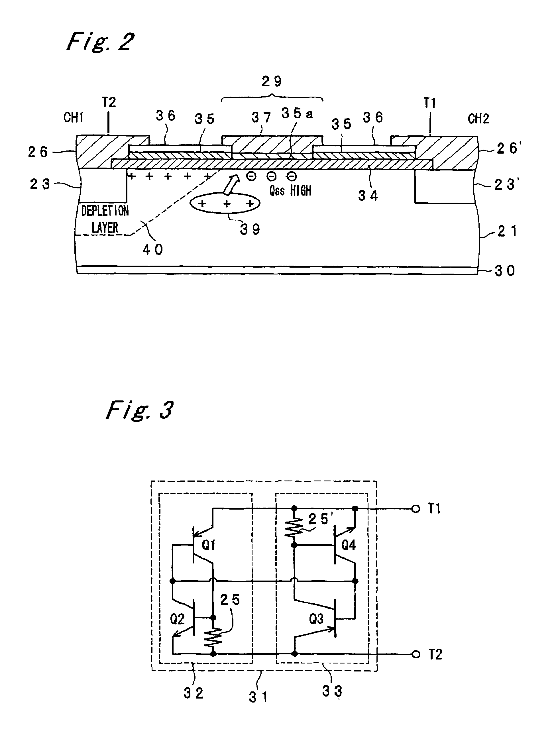
[0168]FIG. 1 is a pattern layout view showing the schematic structure of a bidirectional photothyristor chip of the present embodiment. FIG. 2 is a cross sectional view taken along an arrow line B-B′ in FIG. 1. FIG. 3 is an equivalent circuit view showing the bidirectional photothyristor chip of the present embodiment. It is to be noted that the equivalent circuit view is the same as that of a conventional bidirectional photothyristor chip shown in FIG. 36.

[0169]In the bidirectional photothyristor chip 31, two anode diffusion regions (P type) 22, 22′ are disposed on the surface side of an N-type silicon substrate 21 at positions symmetric with respect to a point of the center of the bidirectional photothyristor chip 31 in such a way that the anode diffusion region 22 is positioned on the left-hand side and the anode diffusion region 22′ is positioned on the right-hand side in FIG. 1. Moreover, two P-gate diffusion regions (P type) 23, 23′ are disposed at positions symmetric with res...

second embodiment

[0182]A bidirectional photothyristor chip in the present embodiment has a structure in which a short diode as the carrier absorption diode is additionally provided to the channel isolation region 29 in the bidirectional photothyristor chip 31 in the first embodiment.

[0183]FIG. 4 is a pattern layout view showing the schematic structure in the bidirectional photothyristor chip in the present embodiment. FIG. 5 is a cross sectional view taken along an arrow line C-C′ in FIG. 4. FIG. 6 is an equivalent circuit view showing the bidirectional photothyristor chip of the present invention.

[0184]An N-type silicon substrate 41, anode diffusion regions 42, 42′, P-gate diffusion regions 43, 43′, cathode diffusion regions 44, 44′, gate resistances 45, 45′, Al electrodes 46, 46′, an Al electrode 47, an Al guard ring 48, an N+ layer 49, a CH1 photothyristor 52 and a CH2 photothyristor 53 in the bidirectional photothyristor chip 51 of the present embodiment are same as the N-type silicon substrate ...

third embodiment

[0190]A bidirectional photothyristor chip in the present embodiment has a structure in which the channel isolation region 29 in the bidirectional photothyristor chip 31 of the first embodiment further extends and is formed across the CH1 and the CH2 along the entire width of the chip.

[0191]FIG. 7 is a pattern layout view showing the schematic structure of a bidirectional photothyristor chip 71 in the present embodiment. It is to be noted that the cross sectional view of a channel isolation region in the bidirectional photothyristor chip 71 is almost identical to that of FIG. 2. Also, its equivalent circuit is identical to that of FIG. 3.

[0192]Anode diffusion regions 72, 72′, P-gate diffusion regions 73, 73′ cathode diffusion regions 74, 74′, gate resistances 75, 75′, Al electrodes 76, 76′ and an Al electrode 77 in the bidirectional photothyristor chip 71 of the present embodiment are same as the anode diffusion regions 22, 22′, the P-gate diffusion regions 23, 23′, the cathode diffu...


PUM


Abstract

Two operation channels CH1 and CH2 of a bidirectional photothyristor chip 31 are disposed away from each other so as not to intersect with each other. In between a P-gate diffusion region 23 on the left-hand side and a P-gate diffusion region 23′ on the right-hand side on an N-type silicon substrate, and in between the CH1 and the CH2, a channel isolation region 29 comprised of an oxygen doped semi-insulating polycrystalline silicon film 35a doped with phosphorus is formed. Consequently, a silicon interface state (Qss) in the vicinity of the channel isolation region 29 on the surface of the N-type silicon substrate increases, so that holes or minority carriers in the N-type silicon substrate are made to disappear in the region. This makes it possible to prevent such commutation failure that when a voltage of the inverted phase is applied to the CH2 side at the point of time when the CH1 is turned off, the CH2 is turned on without incidence of light, and this allows a commutation characteristic to be enhanced.

Description

BACKGROUND OF THE INVENTION[0001]This nonprovisional application claims priority under 35 U.S.C. §119(a) on Patent Application Nos. 2004-075900 and 2005-040675 filed in Japan on Mar. 17, 2004 and Feb. 17, 2005, respectively, the entire contents of which are hereby incorporated by reference.[0002]The present invention relates to a bidirectional photothyristor chip, a light-triggered coupler with use of the same, and a solid state relay (hereinafter abbreviated to SSR) with use of the light-triggered coupler.[0003]Conventionally, there has been a bidirectional photothyristor with the structure shown in FIG. 35 to FIG. 37. It is to be noted that FIG. 35 is a plane view, FIG. 36 is a cross sectional view taken along an arrow line A-A′ of FIG. 35, and FIG. 37 is an equivalent circuit diagram. The bidirectional photothyristor chip 4 is composed of, for example, a CH (channel) 1 photothyristor and a CH2 photothyristor formed on an N-type silicon substrate 1. Such a bidirectional photothyri...

Claims


Application Information

Patent Timeline
Patent Type & Authority Patents(United States)
IPC IPC(8): H01L29/747
CPCH01L31/1113H01R13/688H01H85/0411H01H85/20
Inventor MARIYAMA, MITSURUNAKAJIMA, SATOSHI
Owner SHARP KK
Why Eureka
Try Eureka