Circuit-pattern inspecting apparatus and method

a circuit pattern and inspection apparatus technology, applied in the direction of material analysis using wave/particle radiation, instruments, nuclear engineering, etc., can solve the problems of user who uses these types of inspection apparatus, not necessarily the case, and the individual inspection conditions are complicated and difficult to set, so as to facilitate the process of creating a recipe for an inspection apparatus, the effect of detecting quickly and accurately

Inactive Publication Date: 2008-09-09
HITACHI HIGH-TECH CORP
View PDF6 Cites 25 Cited by
  • Summary
  • Abstract
  • Description
  • Claims
  • Application Information

AI Technical Summary

Benefits of technology

[0035]In accordance with the invention, the process of creating a recipe for an inspection apparatus can be greatly facilitated, thereby allowing a defect to be detected quickly and accurately.

Problems solved by technology

In addition, the setting of the individual inspection conditions and the adjustment of one inspection condition relative to another are complicated and difficult.
As a result, it has not necessarily been the case that any user who uses these types of inspection apparatus can easily and accurately acquire an exterior image of the semiconductor wafer substrate surface or make a decision as to the presence of abnormalities based on such exterior image.
Thus, the apparatuses have not been very easy to operate.
Thus, the screen function has not been fully exploited for the purpose of easy and accurate setting or adjustment of inspection conditions.

Method used


Image

  • Circuit-pattern inspecting apparatus and method
  • Circuit-pattern inspecting apparatus and method
  • Circuit-pattern inspecting apparatus and method

Examples


Embodiment Construction

[0056]In the following, preferred embodiments of the circuit pattern inspection apparatus and method according to the invention will be described with reference to the drawings.

[0057]By the way, the circuit pattern inspection apparatus and method are herein defined as inspection apparatus and method that enable the measurement of the dimensions, the observation, or the inspection of the exterior, of a substrate to be inspected, such as a semiconductor wafer on which a circuit pattern is formed, using light, laser light, or a charged-particle beam.

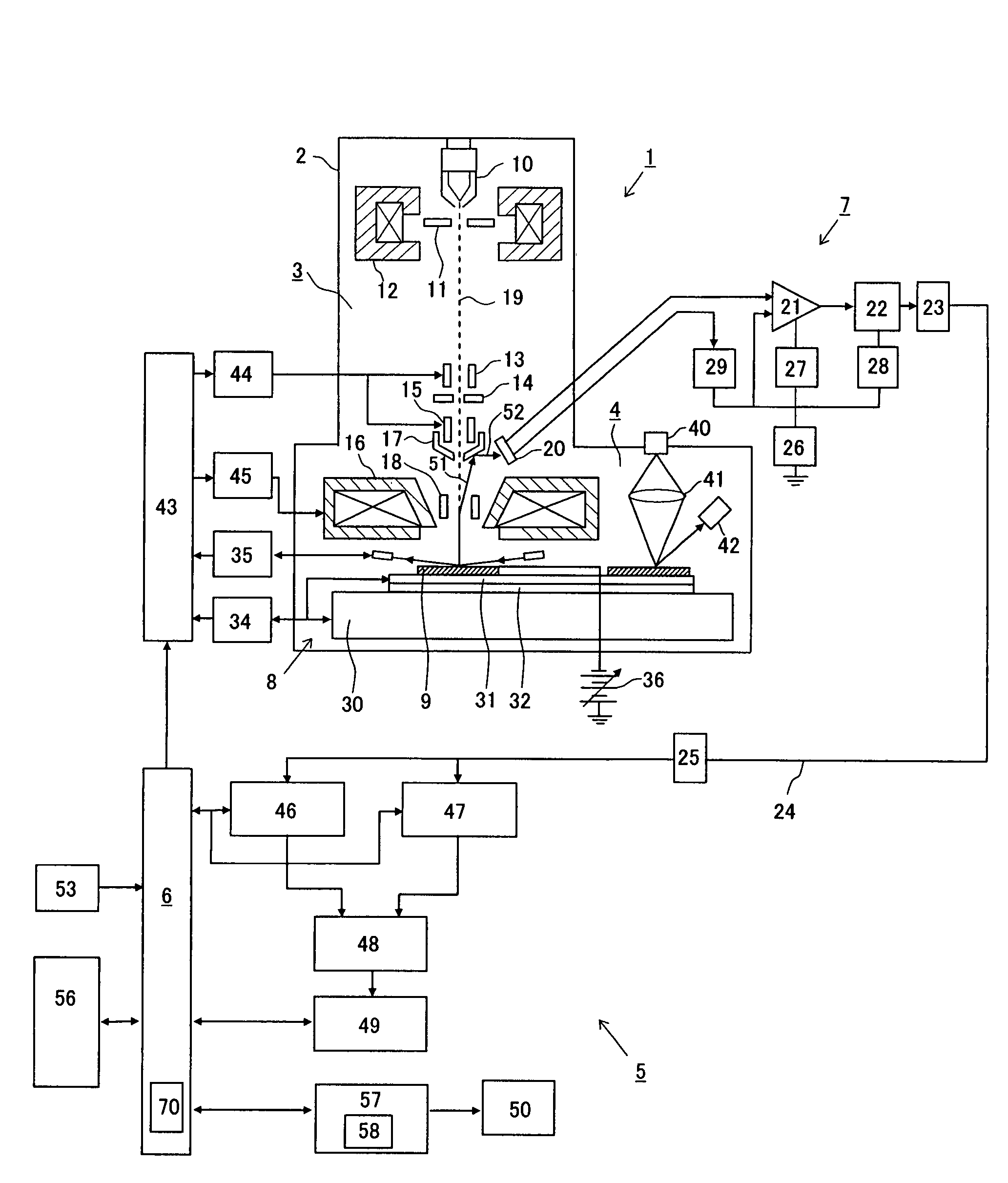
[0058]FIG. 1 shows a block diagram of a circuit pattern inspection apparatus according to an embodiment of the invention.

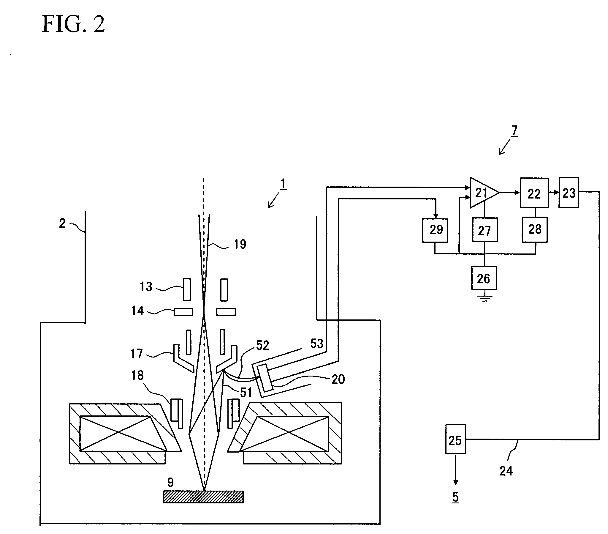
[0059]FIG. 2 shows a partially enlarged view of the inspection apparatus shown in FIG. 1.

[0060]The circuit pattern inspection apparatus 1 of the present embodiment is an example of the aforementioned inspection apparatus using a charged-particle beam.

[0061]Referring to FIG. 1, the circuit pattern inspection apparatus 1 in...


PUM

PropertyMeasurementUnit
energyaaaaaaaaaa
currentaaaaaaaaaa
areaaaaaaaaaaa

Abstract

A circuit pattern inspection apparatus and inspection method facilitate the creation of a recipe and the confirmation of a defect. The apparatus and method employ a dialogue-based operation for the creation of a recipe and the confirmation of a defect. Input items (such as contrast, calibration, etc.) for the recipe creation and their purposes are clarified. Input items (such as clustering, filtering, etc.) for the defect confirmation and their purposes are also clarified. The results obtained on the basis of these inputs are registered in the recipe.

Description

BACKGROUND OF THE INVENTION[0001]1. Field of the Invention[0002]The present invention relates to technologies for inspecting fine circuit patterns for semiconductor devices or LCDs on a substrate, particularly such circuit patterns on a semiconductor wafer. More specifically, the invention relates to such inspecting technologies whereby the circuit patterns formed on a semiconductor wafer are irradiated with light, laser light, or a charged-particle beam to obtain an exterior image of the wafer.[0003]2. Background Art[0004]Semiconductor devices are typically manufactured by repeating the steps of forming a circuit pattern on a semiconductor wafer using a photomask and then transferring the pattern on the semiconductor wafer by lithography and etching. During the manufacture of semiconductor devices, the quality of individual processes including the aforementioned lithography and etching processes, as well as the presence of foreign matter during the manufacturing steps, have a signi...

Claims


Application Information

Patent Timeline
Patent Type & Authority Patents(United States)
IPC IPC(8): G01N21/00
CPCG01N21/95607G01N2021/95676G01N2021/9513
Inventor TAKEDA, MASAYOSHIITO, HIROKAZU
Owner HITACHI HIGH-TECH CORP
Why Eureka
Try Eureka