Photoelectric conversion apparatus and contact-type image sensor

a conversion apparatus and contact-type technology, applied in the field of contact-type image sensors, can solve the problems of large deterioration of image quality, and inability to output negative values, so as to suppress the potential change of a signal storage capacitor, reduce the influence of a change, and improve the effect of image quality

Inactive Publication Date: 2008-09-09
CANON KK
View PDF27 Cites 27 Cited by
  • Summary
  • Abstract
  • Description
  • Claims
  • Application Information

AI Technical Summary

Benefits of technology

[0024]It is therefore an object of the present invention to prevent such a situation that a signal from a pixel in a dark state is output at a level shifted from an originally set level to deteriorate an image quality, and to improve the image quality.
[0055]According to the present invention, it is possible to reduce an influence of a change of an RC time constant of a control line in accordance with the number of pixels irradiated with light, and suppress a potential change of a signal storage capacitor. Accordingly, a photoelectric conversion apparatus can be attained, which can prevent such a situation that a signal from a pixel in a dark state is output at a level shifted from an originally set level to deteriorate an image quality, and to improve the image quality. In particular, this is effective for a contact-type image sensor having plural photoelectric conversion apparatuses mounted thereto.

Problems solved by technology

Thus, the signal whose level is lower than a level originally preset for a dark state is output, whereby a corresponding portion on the image is displayed in black beyond expectations, leading to a deteriorated image quality.
However, the photoelectric conversion apparatuses 401-2 and 401-3 have not received irradiated light at every pixel thereof, so such signals of a negative value are not output.
Howbeit, one of them outputs the signal of a large negative value, so the boundary therebetween is recognized as a step, leading to a much larger deterioration in image quality than that with a single photoelectric conversion apparatus.

Method used


Image

  • Photoelectric conversion apparatus and contact-type image sensor
  • Photoelectric conversion apparatus and contact-type image sensor
  • Photoelectric conversion apparatus and contact-type image sensor

Examples


first embodiment

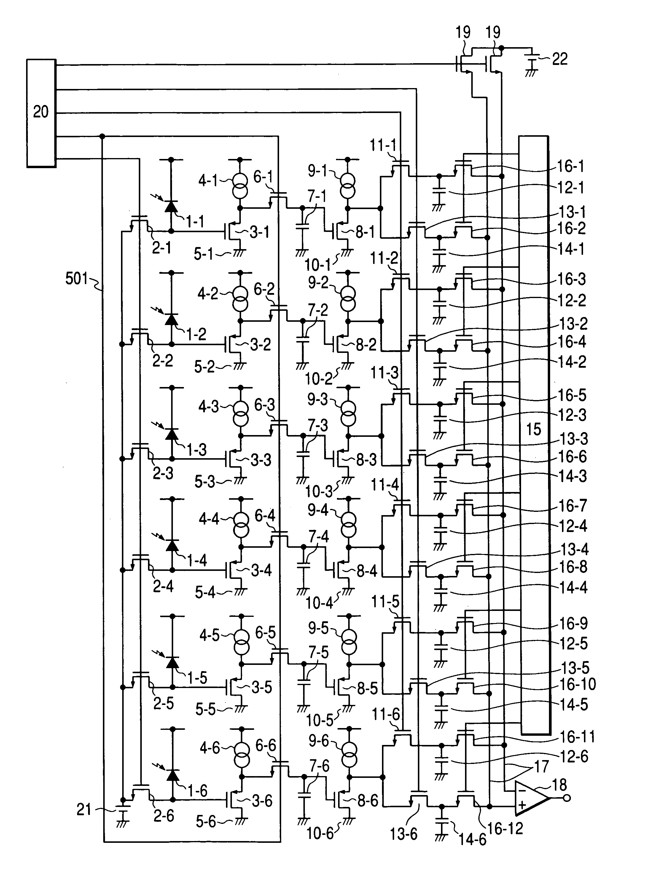
[0074]FIG. 1 is a schematic diagram showing a photoelectric conversion apparatus according to a first embodiment of the present invention.

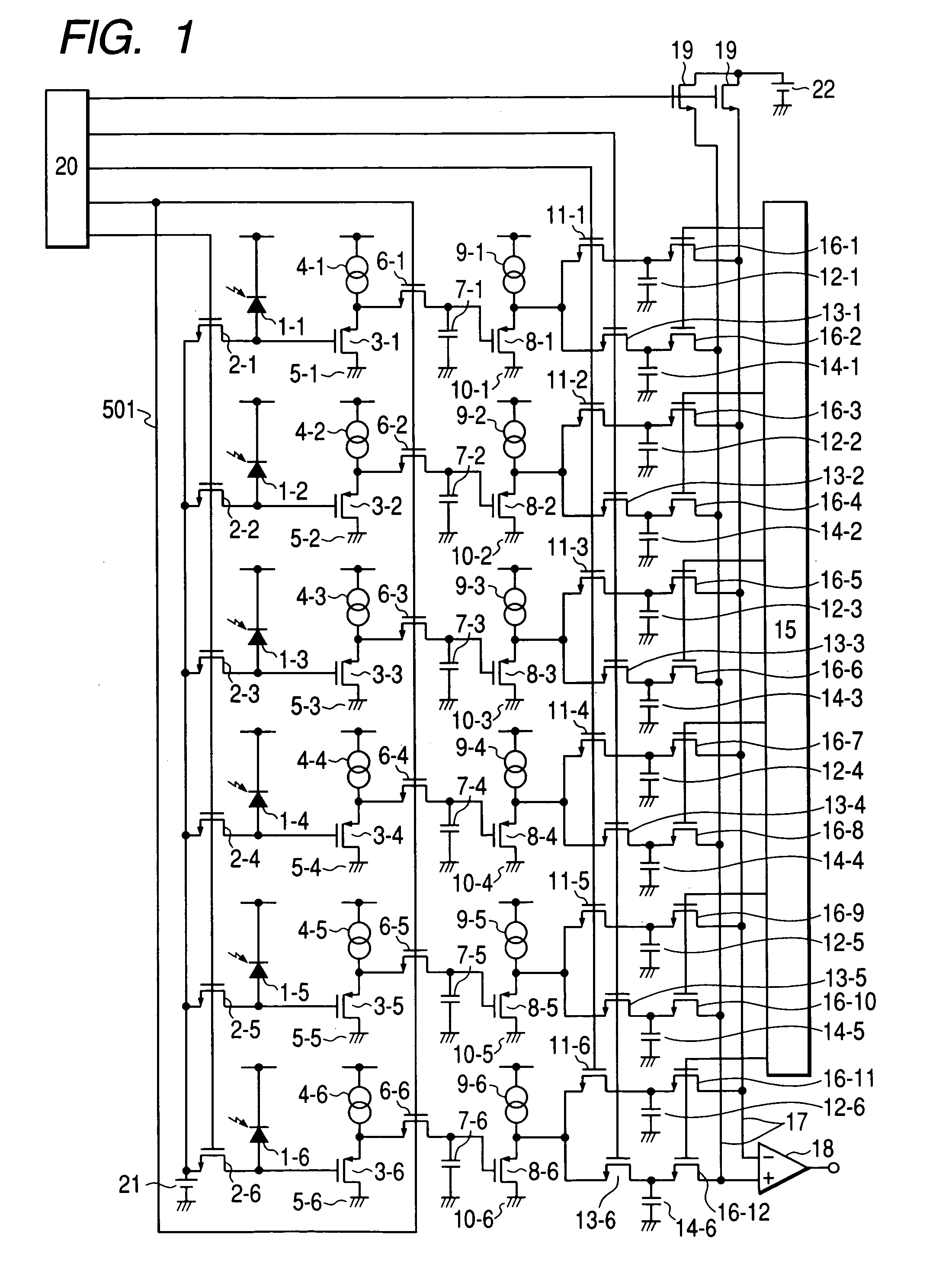
[0075]In FIG. 1, the same members as those in FIG. 14 are denoted by like reference symbols. The photoelectric conversion apparatus of this embodiment is the same as a conventional one in that first transfer MOS transistors 6 are sequentially connected to a single control line, but is different therefrom in that the first transfer MOS transistors 6 are wired with not a given wiring extending from a logic circuit 20 on one side but the given wiring and an additional wiring 501 on both sides.

[0076]As shown in FIG. 1, although the additional wiring 501 involves a resistance component of the wiring itself on its path, there is no gate capacitance component of the MOS transistor involved in the original control line. Thus, a control signal can be transmitted up to a position where the wiring is connected to a first transfer MOS transistor 6-6 of FIG. 1...

second embodiment

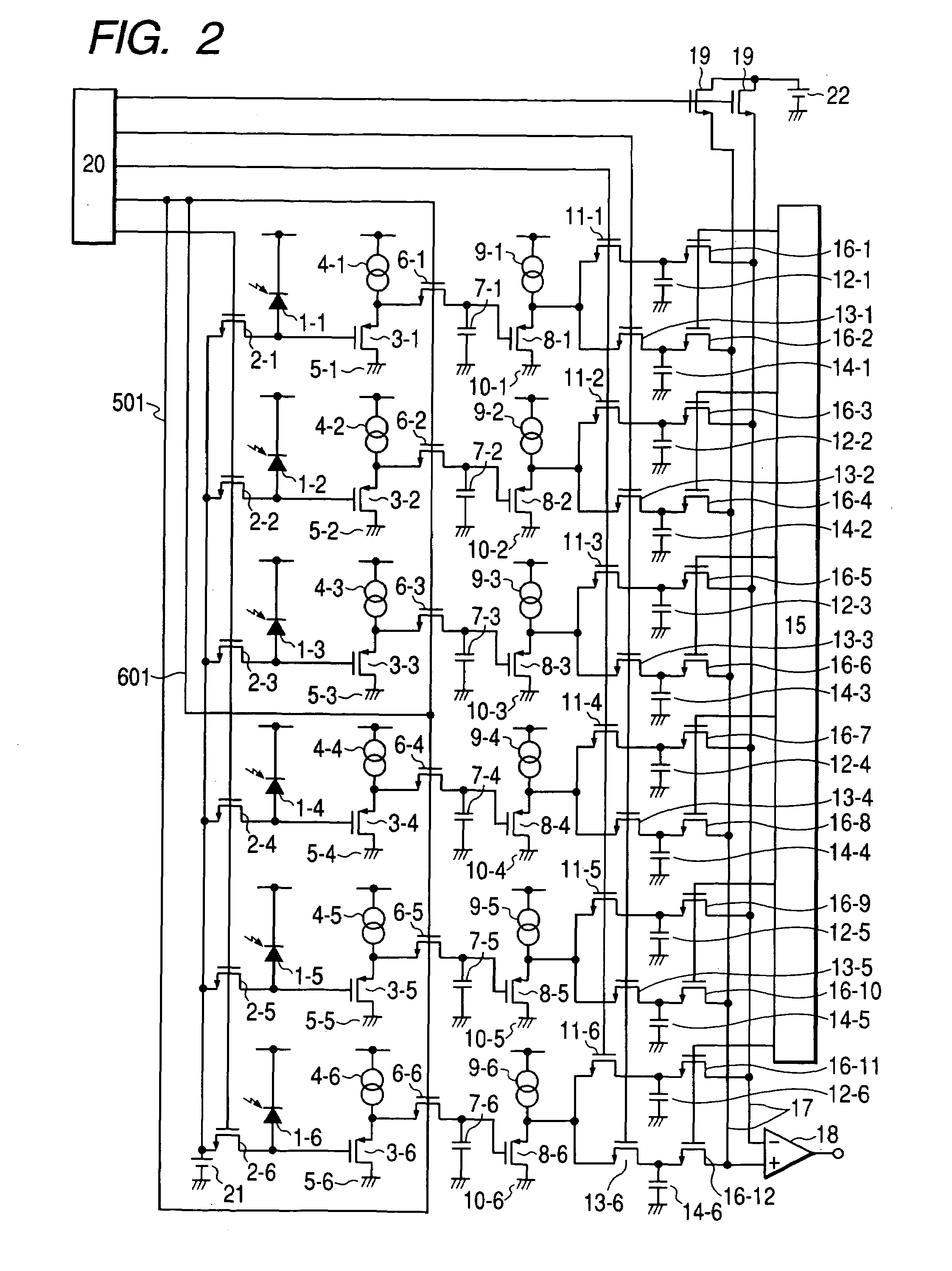
[0079]FIG. 3 is a schematic diagram showing a photoelectric conversion apparatus according to a second embodiment of the present invention.

[0080]In FIG. 3, the same members as those in FIG. 14 are denoted by like reference symbols. The photoelectric conversion apparatus of this embodiment is the same as the first embodiment in that the first transfer MOS transistors 6 are wired with not a given wiring extending from the logic circuit 20 on one side but the given wiring and the additional wiring 501 on both sides, but is different therefrom in that the control signal is subjected to waveform shaping in a buffer circuit 701 immediately before being input to the first transfer MOS transistors 6 at the time of connecting therebetween.

[0081]With this configuration, it is possible to further reduce an influence of an RC time constant change slightly involved in the additional wiring (control line) 501, resulting in a larger improvement effect.

[0082]FIG. 4 shows another example of this emb...

third embodiment

[0085]FIG. 5 is a schematic diagram showing a photoelectric conversion apparatus according to a third embodiment of the present invention.

[0086]In FIG. 5, the same members as those in FIG. 14 are denoted by like reference symbols. In this embodiment, the first transfer MOS transistors 6 are wired with not a given wiring extending from the logic circuit 20 on one side but the given wiring and the additional wiring 501 on both sides. In addition, the control line connected to the first transfer MOS transistors 6 is divided into a control line 901 connected with preceding pixels (one group) and a control line 902 connected with succeeding pixels (the other group) somewhere in the path connecting between the first transfer MOS transistors 6.

[0087]The divided control lines 901 and 902 have terminal ends adjacent to each other on one sides opposite to sides connected to the logic circuit 20 in each group of the first transfer MOS transistors 6.

[0088]Further, although not shown, the divide...


PUM


Abstract

To prevent such a situation that a signal from a pixel in a dark state is output at a level shifted from an originally set level to deteriorate an image quality, and to improve the image quality. A photoelectric conversion apparatus according to the present invention includes: a plurality of photoelectric conversion elements; a plurality of amplifying units for amplifying a signal in accordance with a photo-carrier generated in the photoelectric conversion elements; a plurality of signal holding units for holding output signals from the amplifying units through a plurality of switch units; and a control signal supplying unit for supplying a control signal to the switch units through a control line, in which the control line is sequentially connected to the plurality of switch units and has both ends connected to the control signal supplying units, or a change rate with time of an amplitude of a signal held by the signal holding units is set lower than a change rate with time of am amplitude of the control signal at the time of turning off the switch units.

Description

BACKGROUND OF THE INVENTION[0001]1. Field of the Invention[0002]The present invention relates to a photoelectric conversion apparatus having a photoelectric conversion element and a capacitor element for holding a signal, a contact-type image sensor, and an original image reading apparatus. The contact-type image sensor uses plural photoelectric conversion apparatuses mounted thereto to read an original image by receiving light reflected by an original surface to be read.[0003]2. Related Background Art[0004]FIG. 14 is a schematic diagram of a conventional photoelectric conversion apparatus.[0005]In FIG. 14, a circuit of a 6-pixel linear sensor is shown as an example. The respective pixels are arranged in line. Reference numeral 1 denotes a photoelectric conversion element such as a photodiode; a hole storage type photodiode is used by way of example herein (note that the photoelectric conversion element 1 is assigned with sub-numbers like 1-1, 1-2, . . . for each pixel; the same app...

Claims


Application Information

Patent Timeline
Patent Type & Authority Patents(United States)
IPC IPC(8): H04N1/46H04N1/028H04N3/14H04N5/361H04N5/374H04N5/378
CPCH04N3/155H04N25/701H04N25/771H04N25/745
Inventor KOCHI, TETSUNOBUYAMAZAKIKOZUKA, HIRAKU
Owner CANON KK
Why Eureka
Try Eureka