Noncontact localized electrochemical deposition of metal thin films

a metal thin film, noncontact technology, applied in the direction of electrolysis components, coatings, printed circuit manufacturing, etc., can solve the problems of dropping in potential towards the center of the semiconductor wafer, unneeded metal portions must be removed by polishing,

Active Publication Date: 2008-10-14
MICRON TECH INC
View PDF12 Cites 10 Cited by
  • Summary
  • Abstract
  • Description
  • Claims
  • Application Information

AI Technical Summary

Benefits of technology

[0007]The electroplating system may also include a chuck or platen on which a substrate having a conductive surface upon which metal features are to be selectively plated is supported. The electrode assembly is supported using an electrode support over the chuck or platen in selected alignment in the horizontal (X-Y) plane and rotationally about a vertical (Z) axis perpendicular thereto with the substrate and, more specifically, with semiconductor die locations thereon. The conductive surface of the substrate may be positioned in close proximity to the electrode assembly, such as from approximately 0.1 mm to approximately 1 cm away from the electrode assembly and aligned therewith to cause the pattern of plated metal features to be precisely located and configured.

Problems solved by technology

One disadvantage with the damascene process is that since the entire surface of the semiconductor wafer is covered with the metal, undesired portions of the metal must be removed by polishing.
A second disadvantage is that the metal is deposited nonuniformly on the semiconductor substrate because the electrodes are connected to edges of the semiconductor wafer, which causes a drop in potential towards the center of the semiconductor wafer.

Method used


Image

  • Noncontact localized electrochemical deposition of metal thin films
  • Noncontact localized electrochemical deposition of metal thin films
  • Noncontact localized electrochemical deposition of metal thin films

Examples


Embodiment Construction

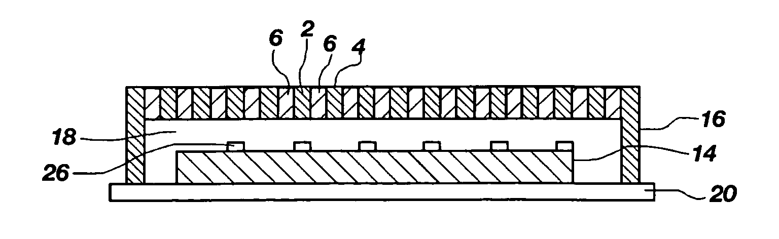
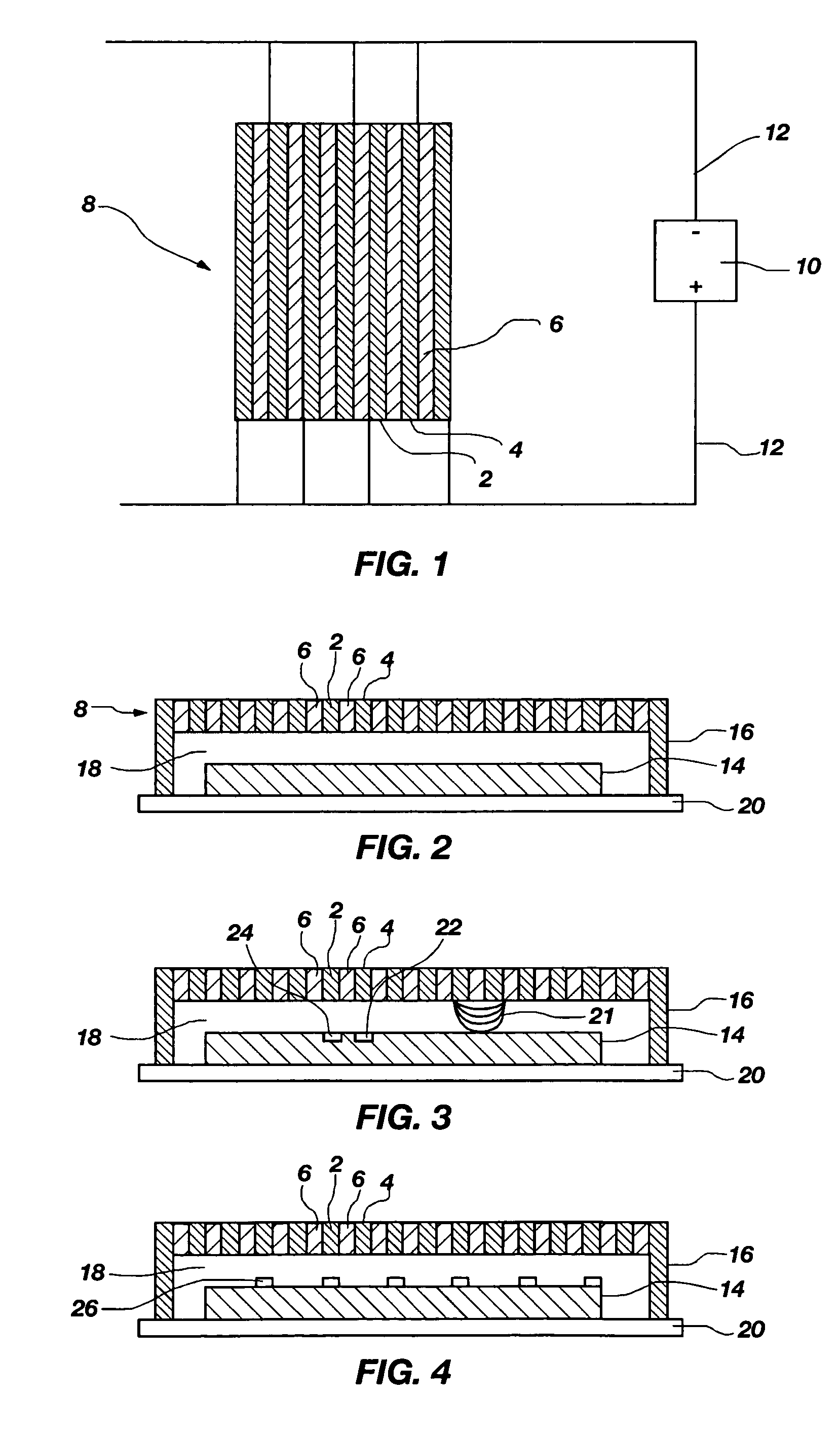
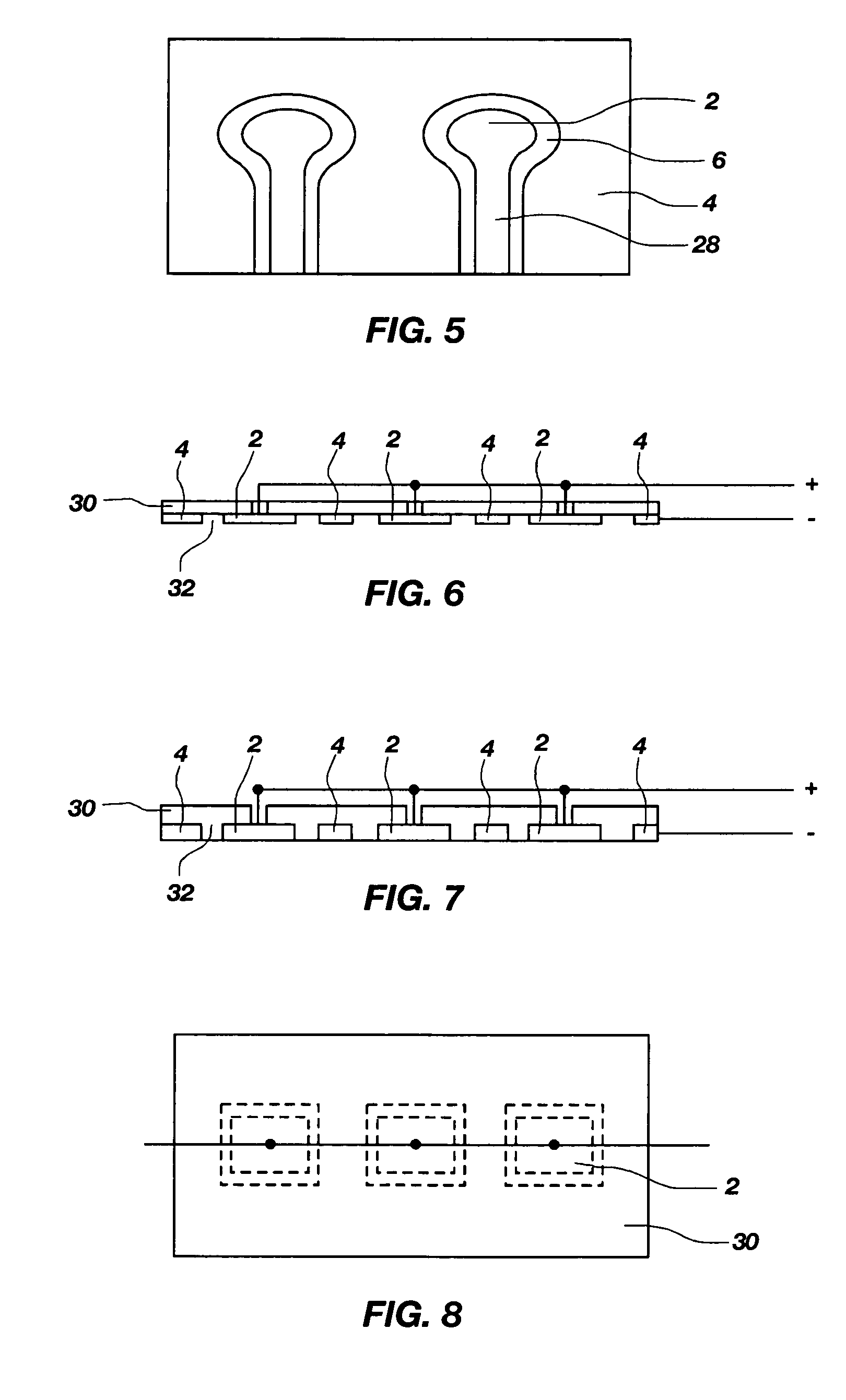
[0014]A metal film is deposited on a conductive surface of a substrate without electrical contact between the conductive surface and electrodes of an electrode assembly. As such, the metal film is selectively deposited on the conductive surface of the substrate in the form of discrete metal features by noncontact electrochemical deposition. The metal features may be deposited on the conductive surface of the substrate when a fringe electric field, which is generated by applying a voltage across a plurality of positive electrodes and negative electrodes that are connected in series, passes through the conductive surface of the substrate. Conductive polymers or conductive salts may also be deposited on the conductive surface of the substrate rather than the metal film. As shown in FIG. 1, the positive electrodes 2 and the negative electrodes 4 are adjacent to one another and are separated by an interposed insulating material 6. The dimensions of the positive electrodes 2, the negative...


PUM

PropertyMeasurementUnit
voltageaaaaaaaaaa
voltageaaaaaaaaaa
voltageaaaaaaaaaa

Abstract

A method of selectively electroplating metal features on a semiconductor substrate having a conductive surface. An electrode assembly that includes a plurality of adjacent, mutually spaced and electrically isolated electrodes connected in series so as to be oppositely polarized when a voltage is applied thereacross is positioned over the substrate and an electrolyte solution is applied to the conductive surface. The electrode assembly and the conductive surface may be positioned in close proximity to, but without contacting, one another. A voltage is applied to the electrode assembly, which causes a metal film to selectively form on portions of the conductive surface that are positioned beneath an electrode exhibiting a positive polarity and, thus, negatively charged. Portions of the conductive surface positioned beneath electrodes exhibiting a negative polarity remain unplated. A DC power supply may be employed, the electrode polarity in such case being fixed or, alternatively, an AC power supply may be employed so as to cyclically vary electrode polarity and cause metal deposition beneath each electrode. An electroplating system is also disclosed.

Description

FIELD OF THE INVENTION[0001]The present invention relates to electrochemical deposition of a metal film. More specifically, the present invention relates to a noncontact method of selectively electrochemically depositing metal features of a desired size and shape and at desired locations on a surface of a substrate, such as a semiconductor substrate.BACKGROUND OF THE INVENTION[0002]To fabricate integrated circuits, multiple conductive layers are formed on semiconductor substrates to provide electrical contact between conductive components on the semiconductor devices. Since the dimensions of semiconductor devices have dropped below one micron design rules, the conductive layers are used to accommodate higher densities. The conductive layers are typically metal layers or metal features that are formed by chemical vapor deposition (“CVD”), physical vapor deposition (“PVD”), atomic layer deposition (“ALD”), or other electrodeposition techniques, such as electroplating or electroless de...

Claims


Application Information

Patent Timeline
Patent Type & Authority Patents(United States)
IPC IPC(8): C25D5/02
CPCC25D5/18C25D17/10H01L21/2885C25D17/001C25D17/12C25D7/123C25D17/002
Inventor RAMARAJAN, SURESHLEE, WHONCHEE
Owner MICRON TECH INC
Why Eureka
Try Eureka