Electrical connections in microelectromechanical devices

a micro-electromechanical and electrical connection technology, applied in the direction of coupling contact member, coupling device connection, instrument, etc., can solve the problems of electrical signals (voltages) not being delivered to or applied to the target elements, and the difficulty of electrical connection to the mems devi

Inactive Publication Date: 2008-10-14
TEXAS INSTR INC
View PDF11 Cites 61 Cited by
  • Summary
  • Abstract
  • Description
  • Claims
  • Application Information

AI Technical Summary

Problems solved by technology

The insulating material, however, may isolate the electrically conductive layers that are desired to be electrically connected; and in turn bringing about electrical connection difficulties to the MEMS devices.
Because of the electrical isolation of the electrically conductive layers, electrical signals (voltages) are not be able to be delivered to or applied on the target elements, such as the mirror plate of the micromirror devices.

Method used


Image

  • Electrical connections in microelectromechanical devices
  • Electrical connections in microelectromechanical devices
  • Electrical connections in microelectromechanical devices

Examples


Embodiment Construction

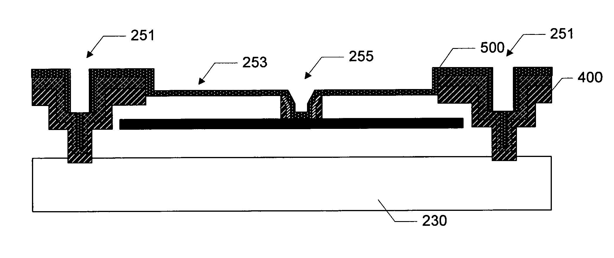
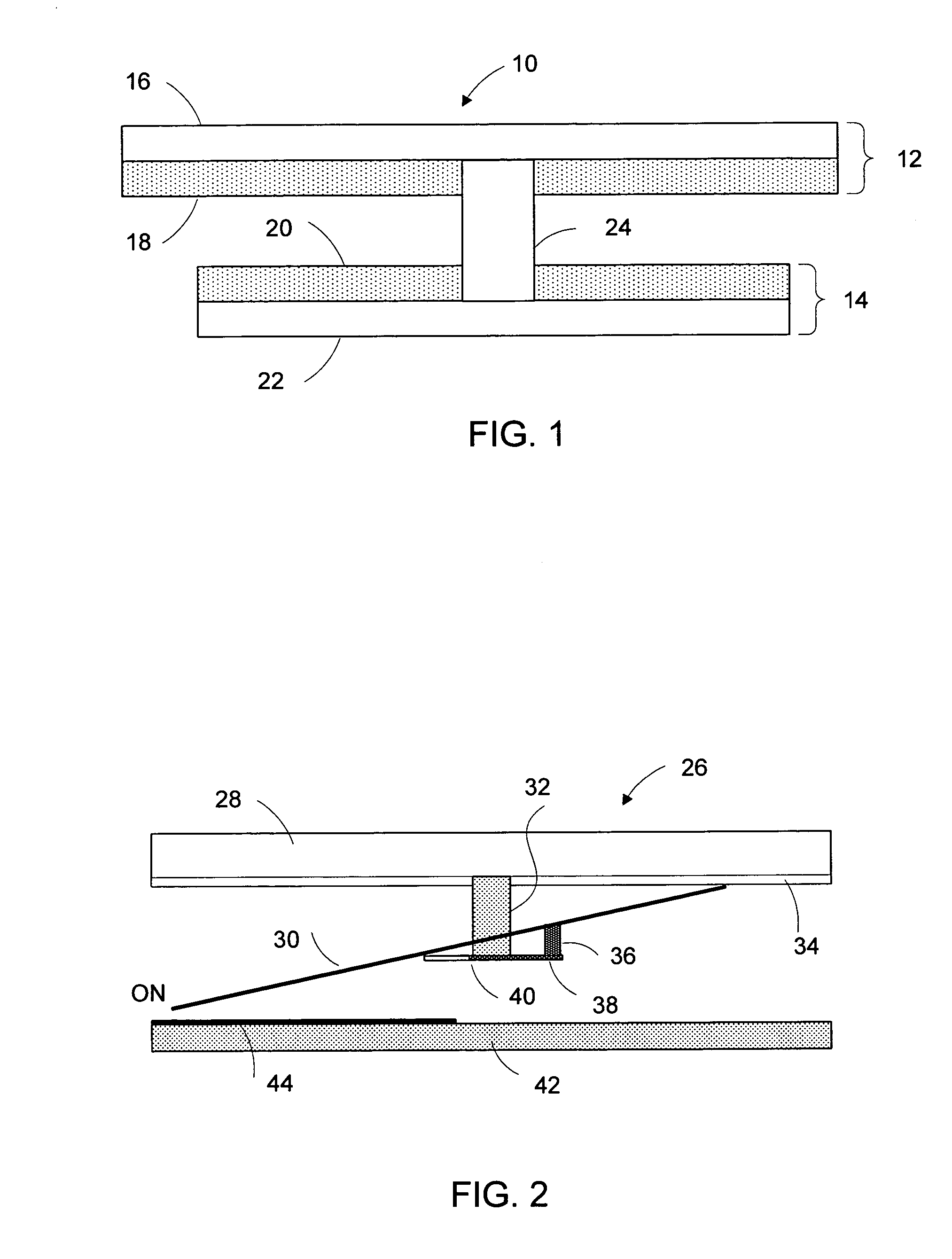
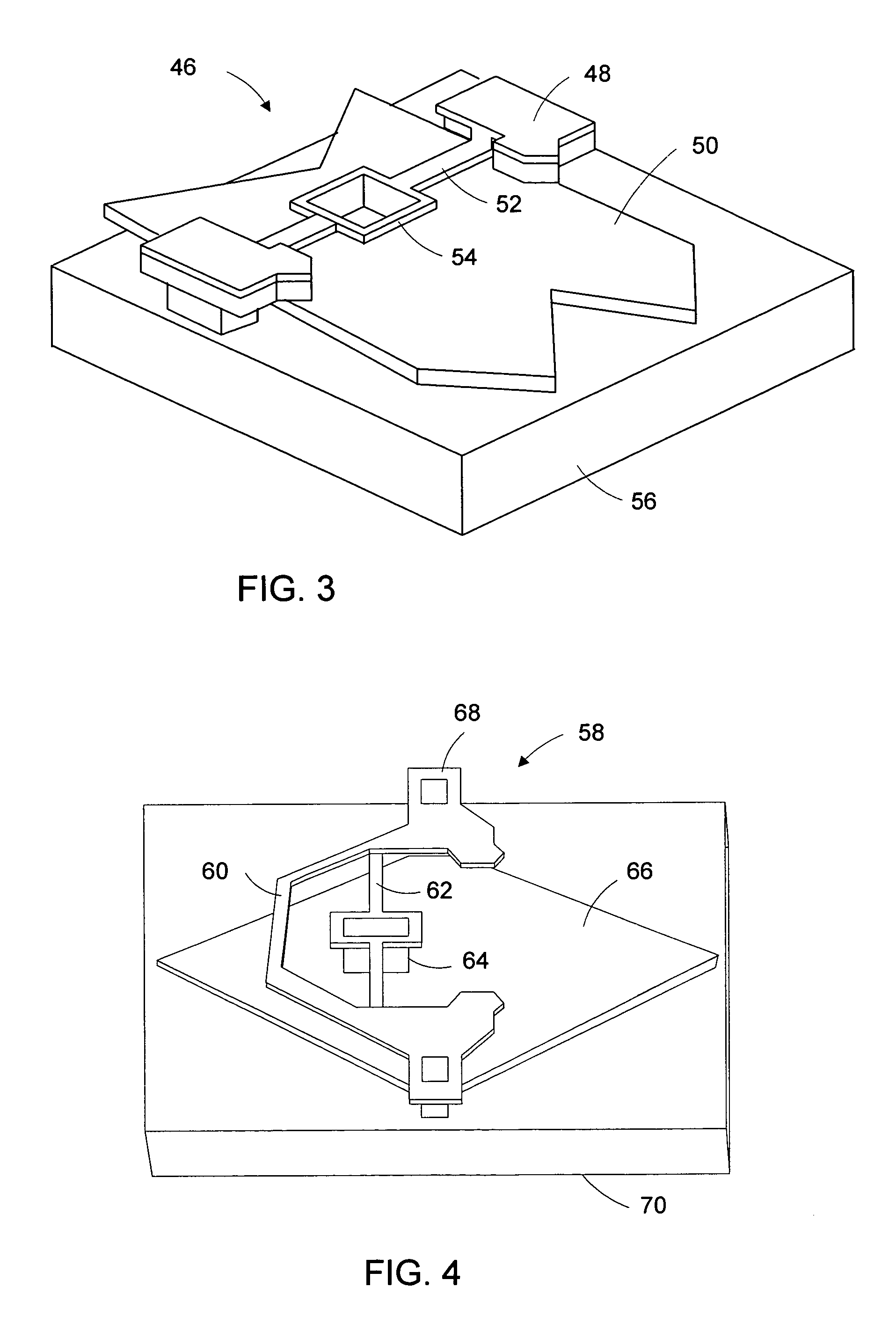
[0027]Turning to the drawings, FIG. 1 illustrates a cross-sectional view of a portion of a MEMS device. MEMS device 10 comprises element 12 and 14 each or both can be the electrical or mechanical elements. Proper operations of the MEMS device require electrical connection between electrically conductive layers 16 in element 12 and 22 in element 14. However, the electrically conductive layers 16 and 22 are electrically isolated by an electrically insulating layer between layers 16 and 22, such as electrically insulating layer 18 in element 12 or layer 20 in element 14 or both. The electrically insulating layers are provided for many reasons, such as to improve the mechanical properties of elements 12 and / or 14, to prevent diffusion between sacrificial materials and layers 16 and / or 22 during fabrication, and to comply with other particular requirements. To enable the desired electrical connection between layers 16 and 22 while keeping the intervening insulating layer(s) therebetween,...


PUM

PropertyMeasurementUnit
reflectivityaaaaaaaaaa
temperaturesaaaaaaaaaa

Abstract

A micromirror device and a method of making the same are disclosed herein. The micromirror device comprises a mirror plate, hinge, and post each having an electrically conductive layer. One of the hinge, mirror plate, and post further comprises an electrically insulating layer. To enable the electrical connections between the conducting layers of the hinge, mirror plate, and post, the insulating layer is patterned.

Description

CROSS-REFERENCE TO RELATED APPLICATIONS[0001]This patent application is a continuation-in-part of U.S. patent application Ser. No. 10 / 365,951 filed Feb. 12, 2003 now U.S. Pat. No. 6,952,302, the subject matter being incorporated herein by reference in entirety.TECHNICAL FIELD OF THE INVENTION[0002]The present invention is related generally to the art of microelectromechanical devices, and, more particularly, to electrical connections between conductive members of the microelectromechanical devices and methods for making the same.BACKGROUND OF THE INVENTION[0003]Microelectromechanical systems (MEMS) are devices with characteristic dimensions of hundreds of microns or less, which integrate electrical and mechanical elements through microfabrication technology. The electrical and mechanical elements comprise electrically conductive layers on or through which external electrical signals can be applied or delivered such that operations of the electrical and / or mechanical elements can be ...

Claims


Application Information

Patent Timeline
Patent Type & Authority Patents(United States)
IPC IPC(8): G02B26/00G02B26/08
CPCG02B26/0833G02B26/0841Y10T29/49155
Inventor DOAN, JONATHAN C.PATEL, SATYADEV R.DUBOC, JR., ROBERT M.
Owner TEXAS INSTR INC
Why Eureka
Try Eureka