Deep alignment marks on edge chips for subsequent alignment of opaque layers

a technology of alignment marks and edge chips, which is applied in the direction of semiconductor devices, semiconductor/solid-state device details, electrical devices, etc., can solve the problems of difficult to use alignment marks to align a subsequently deposited opaque layer, additional steps must be taken, and depressions that are unusable for alignment, etc., to achieve the effect of improving alignmen

Inactive Publication Date: 2008-10-28
POLARIS INNOVATIONS LTD
View PDF55 Cites 13 Cited by
  • Summary
  • Abstract
  • Description
  • Claims
  • Application Information

AI Technical Summary

Benefits of technology

[0017]Advantages of embodiments of the present invention include providing improved methods of patterning opaque material layers of semiconductor devices. Because the deep alignment marks formed in the via level insulating layer are not subjected to a CMP process and are relatively deep, e.g., about 8,000 Angstroms or more, and about 1 μm or more in one embodiment, the depressions formed in the opaque material layer are clearly visible and advantageously, can be used for alignment in the lithography process to expose alignment marks in an underlying metallization layer. The exposed alignment marks in the metallization layer may then be used to align the lithography process to pattern the opaque material layer. The deep alignment marks are formed in unused areas or areas of incomplete die on the workpiece kerf region, making use of wasted space on the workpiece and providing improved alignment. The kerf region portions of the workpiece may simply be discarded after the singulation process to separate the individual die. Embodiments of the present invention are particularly beneficial when used with semiconductor devices having a top surface with no topography, or very little topography (e.g., having shallow features or alignment marks).

Problems solved by technology

However, many conductive layers are optically opaque, and thus additional steps must be taken to align them.
However, if the recessed alignment marks are formed in a damascene formed layer, such as conductive lines or vias formed in an insulating layer, and the insulating layer is subjected to a chemical mechanical polish (CMP) process, (as is typical to remove excess conductive material from the top surface of the insulating layer to form the conductive lines or vias) the edges of the alignment marks become eroded by the CMP process, and thus the edges are not sharp.
This makes it difficult to use the alignment marks to align a subsequently deposited opaque layer, because the depressions transferred to the topography of the opaque layer are not as visible on the top surface of the opaque layer.
There are other problems with using a CMP process over recessed alignment marks.
In addition, the deposition of opaque layers over such alignment marks give rise to jagged edges in the depressions in the topography of the opaque layer over the alignment marks, making the depressions unusable for alignment.
Furthermore, the CMP slurry materials left in the alignment marks can react with some materials used in subsequent etch processes, such as chlorine or fluorine, causing the alignment marks to explode, making them unusable as alignment marks.
This creates foreign materials all over the chip, leads to delamination of layers, and thus adversely affects the device performance and reduces yield.
However, copper is difficult to etch, and damascene processes using CMP processes are often used to form copper lines and metallization alignment marks in conductive line and via levels.

Method used


Image

  • Deep alignment marks on edge chips for subsequent alignment of opaque layers
  • Deep alignment marks on edge chips for subsequent alignment of opaque layers
  • Deep alignment marks on edge chips for subsequent alignment of opaque layers

Examples


Embodiment Construction

[0026]The making and using of the presently preferred embodiments are discussed in detail below. It should be appreciated, however, that the present invention provides many applicable inventive concepts that can be embodied in a wide variety of specific contexts. The specific embodiments discussed are merely illustrative of specific ways to make and use the invention, and do not limit the scope of the invention.

[0027]The present invention will be described with respect to preferred embodiments in a specific context, namely an MRAM device. The invention may also be applied, however, to other resistive memory devices or semiconductor devices with opaque material layers.

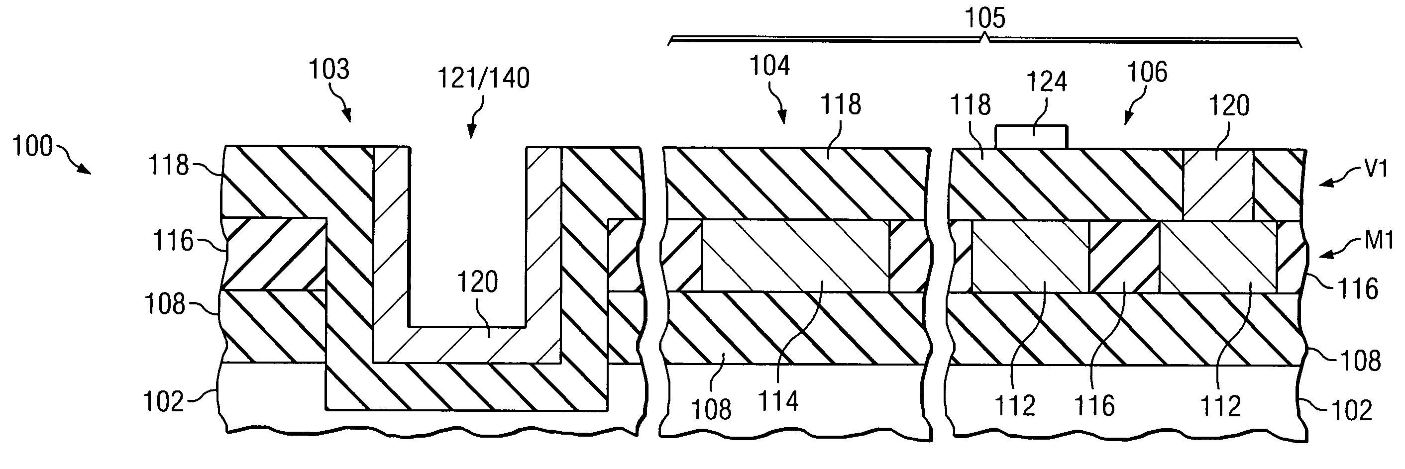
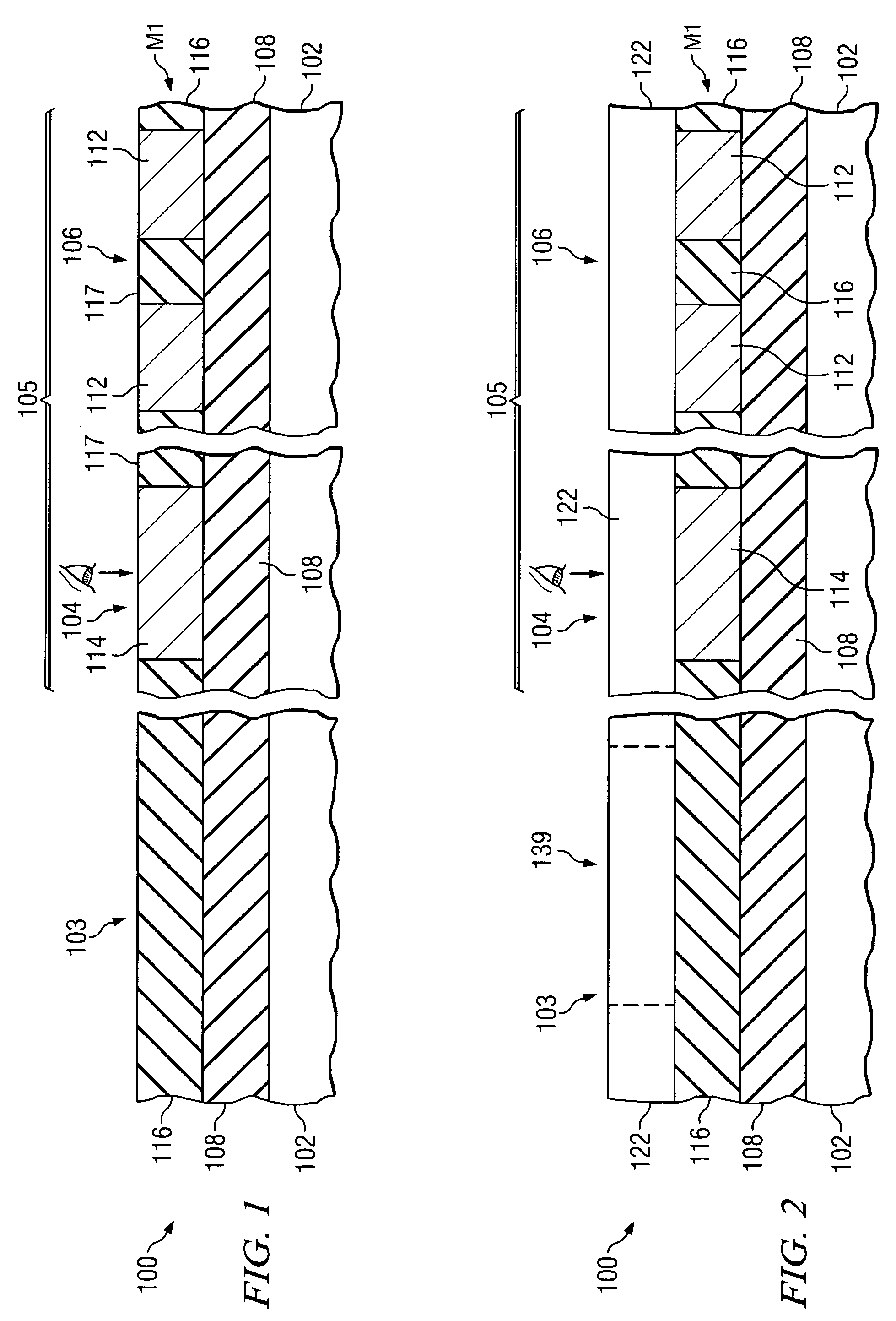
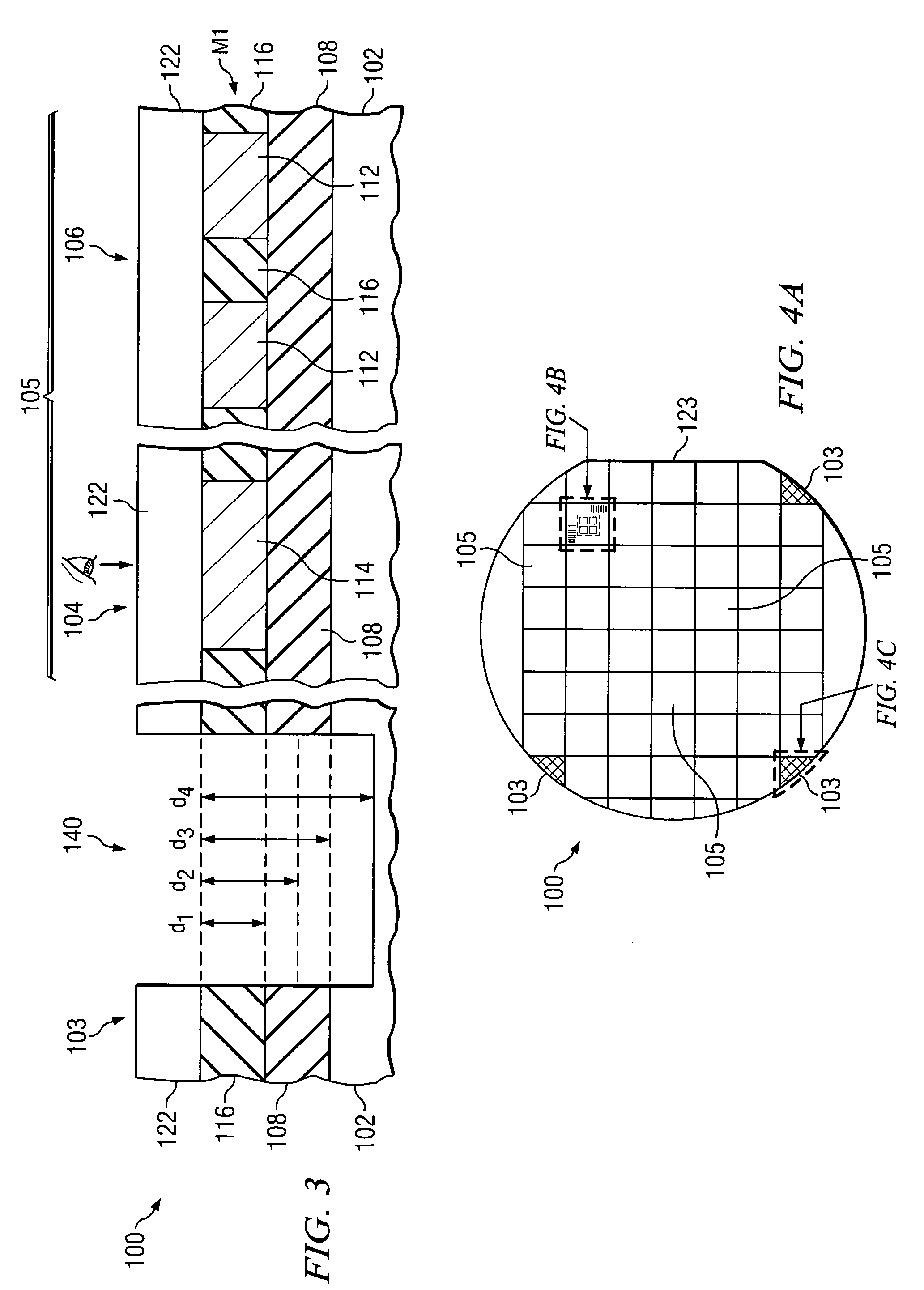
[0028]Embodiments of the present invention provide novel methods of forming deep alignment marks in kerf regions of a workpiece, and using the deep alignment marks for alignment when opening up areas of other alignment marks, e.g., in a metallization layer, so that the other alignment marks can be used to pattern opaque...


PUM


Abstract

A method of forming alignment marks on edge chips in a kerf region of a semiconductor workpiece. The alignment marks are formed in at least one material layer of the semiconductor device. The alignment marks are formed using a separate lithography mask, and may extend into lower layers, including the workpiece, of the semiconductor device. An opaque material layer is deposited, and depressions are formed in the opaque layer over the deep alignment mark trenches. The depressions in the opaque material layer are used to align a lithography process to open the opaque material layer over alignment marks in an underlying metallization layer. The alignment marks in the metallization layer are then used to align the lithography process used to pattern the opaque material layer.

Description

CROSS-REFERENCE TO RELATED APPLICATIONS[0001]This application relates to the following and commonly assigned patent application: Ser. No. 10 / 899,253 filed on Jul. 26, 2004, now U.S. Pat. No. 7,223,612 entitled, “Alignment of MTJ Stack to Conductive Lines in the Absence of Topography,” which application is hereby incorporated herein by reference.TECHNICAL FIELD[0002]The present invention relates generally to the fabrication of semiconductor devices, and more particularly to the alignment of opaque material layers of semiconductor devices.BACKGROUND[0003]Generally, semiconductor devices are fabricated by deposited a plurality of insulating, conductive and semiconductive material layers over a substrate or workpiece, and patterning the various material layers to form integrated circuits and electronic elements thereon. Each layer is typically aligned to an underlying material layer using alignment marks. The tools used to fabricate semiconductor devices visually locate the alignment ma...

Claims


Application Information

Patent Timeline
Patent Type & Authority Patents(United States)
IPC IPC(8): H01L21/46H01L21/301H01L21/76H01L21/78H01L21/311
CPCH01L23/544H01L27/222H01L2223/5442H01L2223/54466H01L2223/5448H01L2924/0002H01L2223/54493H01L2924/00H10B61/00
Inventor SARMA, CHANDRASEKHARKASKO, IHAR
Owner POLARIS INNOVATIONS LTD
Why Eureka
Try Eureka