

Through silicon via chip stack package capable of facilitating chip selection during device operation
- Summary
- Abstract
- Description
- Claims
- Application Information
AI Technical Summary
Benefits of technology
Problems solved by technology
Method used
Image

Examples
Embodiment Construction
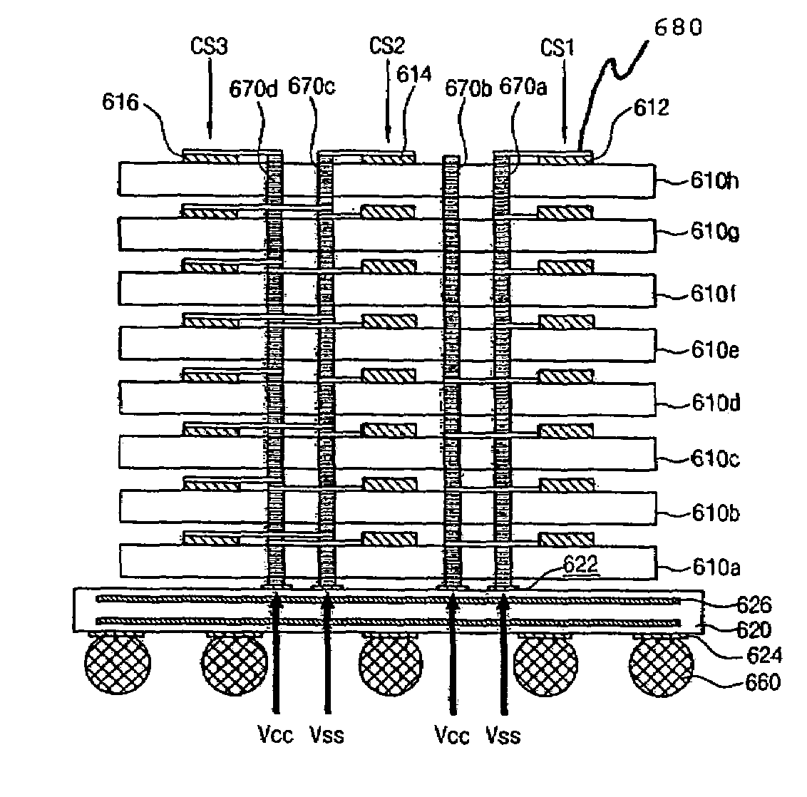
[0035]A preferred embodiment of the present invention is directed to a chip stack package in which a TSV is formed in each of the chips having at least two chip selection pads and at least two rewirings for connecting the TSV and the chip selection pads. The chips are stacked using the TSV. At this time, the rewirings in each chip are formed so that the stacked chips have connection structures between the TSVs and the chip selection pads, which are different from each other.
[0036]By doing this, since the stacked chips have connection structures between the TSVs and the chip selection pads which are different from one another, it is possible to facilitate a chip selection even during the device is operated by making an applied signal to the TSV including the rewiring different in each of the chips.
[0037]Therefore, in an embodiment of the present invention, since there are an advantage that a chip selection is facilitated as well as advantages that a size and a height of a package are...
PUM
 Abstract
Description
Claims
Application Information