Output controller for controlling data output of a synchronous semiconductor memory device

a technology of output controller and memory device, which is applied in the direction of digital storage, pulse automatic control, instruments, etc., can solve the problems of insufficient speed of synchronous memory device, inability to perform process within the memory device, and inability to meet the speed requirement of high-speed system, etc., to reduce unnecessary current consumption

Active Publication Date: 2008-11-04
SK HYNIX INC
View PDF16 Cites 6 Cited by
  • Summary
  • Abstract
  • Description
  • Claims
  • Application Information

AI Technical Summary

Benefits of technology

[0029]It is, therefore, an object of the present invention to provide an output controller for reducing unnecessary current consumption.

Problems solved by technology

However, the SDR synchronous memory device is insufficient to satisfy the speed requirement of a high-speed system.
Because the DDR memory device has to receive or output two data bits during one clock cycle, a data access method employed in the conventional synchronous memory device can no longer be used.
However, it is difficult to perform the process within the memory device.
However, due to the delay time of the clock signal, which inevitably occurs during the internal processing, the data output cannot be accurately synchronized with the rising and falling edges of the external clock.
As a result, unnecessary current consumption is occurs.

Method used


Image

  • Output controller for controlling data output of a synchronous semiconductor memory device
  • Output controller for controlling data output of a synchronous semiconductor memory device
  • Output controller for controlling data output of a synchronous semiconductor memory device

Examples


first embodiment

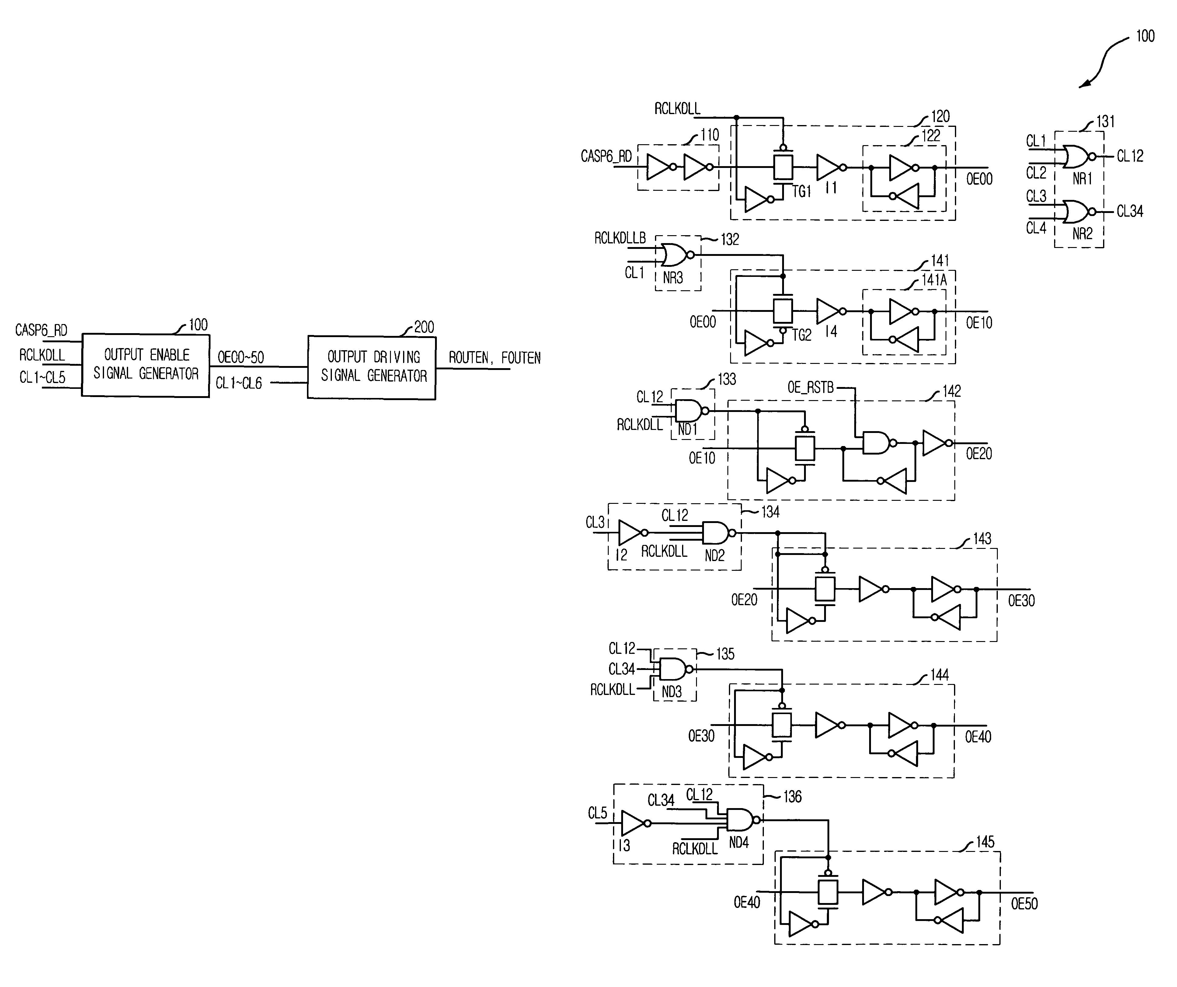
[0044]FIG. 5 is a detailed circuit diagram of the output enable signal generator 100 shown in FIG. 4 in accordance with the present invention. Particularly, FIG. 5 shows the output enable signal generator 100 which is operated in synchronization with a rising delay locked loop (DLL) clock RCLKDLL. The output enable signal generator 100 operated in synchronization with a falling DLL clock FCLKDLL is the same circuit structure shown in FIG. 5, except that the output enable signals are activated half clock later.

[0045]As shown, the output enable signal generator 100 includes an inverter chain 110, an initial synchronizing unit 120, a control unit 131 to 136, and first to fifth synchronizing units 141 to 145.

[0046]The inverter chain 110 delays and transfers the read CAS signal CASP6_RD to the initial synchronizing unit 120. The initial synchronizing unit 120 outputs a first output enable signal OE00 by synchronizing an output signal of the inverter chain 110 with the rising DLL clock RC...

second embodiment

[0071]FIG. 6 is a circuit diagram of the output enable signal generator 100 shown in FIG. 4 in accordance with the present invention.

[0072]The output enable signal generator 100 in accordance with the second embodiment of the present invention includes an inverter chain 150, an initial synchronizing unit 155, a control unit 171 to 175, and first to fifth synchronizing units 161 to 165.

[0073]The inverter chain 150 delays and transfers the read CAS signal CASP6_RD to the initial synchronizing unit 155. The initial synchronizing unit 155 outputs a first output enable signal OE00 by synchronizing an output signal of the inverter chain 150 with the rising DLL clock RCLKDLL. The control unit 171 to 175 receives an inverted rising DLL clock RCLKDLLB and the CAS latency information signals CL1 to CL5, and generates first to fifth control signals. The first to fifth synchronizing units 161 to 165 connected in series receive output signals of the respective previous stages and output the outp...


PUM


Abstract

An output controller includes: an output enable signal generator for generating corresponding ones among a plurality of output enable signals based on a preset column address strobe (CAS) latency, each of the output enable signals having information relating to a delay time from an activation timing of a CAS signal; and an output driving signal generator for receiving the plurality of output enable signals corresponding to the preset CAS latency and outputting rising and falling output driving signals for controlling an output timing of data.

Description

FIELD OF THE INVENTION[0001]The present invention relates to a semiconductor memory device, and more particularly to an output controller for controlling a data output of a semiconductor memory device.DESCRIPTION OF RELATED ARTS[0002]As semiconductor memory devices are highly integrated, many attempts have been made to increase their operating speed. To achieve this purpose, synchronous memory devices which operate in synchronization with an external clock have been introduced.[0003]A single data rate (SDR) synchronous memory device inputs and outputs one data bit via one data pin in synchronization with a rising edge of the external clock during one clock cycle.[0004]However, the SDR synchronous memory device is insufficient to satisfy the speed requirement of a high-speed system. Thus, a double data rate (DDR) synchronous memory device which processes two data bits during one clock cycle has been proposed.[0005]In the DDR synchronous memory device, two data bits are consecutively ...

Claims


Application Information

Patent Timeline
Patent Type & Authority Patents(United States)
IPC IPC(8): G11C8/18H03L7/00
CPCG11C7/1051G11C7/1066G11C7/1069G11C7/22G11C7/222G11C29/022G11C29/023G11C29/50G11C29/50012G11C11/401G11C11/4076G11C11/4096
Inventor CHOI, HOON
Owner SK HYNIX INC
Why Eureka
Try Eureka