Carbon nanotube deposition with a stencil

a carbon nanotube and stencil technology, applied in the field of carbon nanotube deposition, can solve the problems of increasing production cost, difficult to achieve uniform film properties over a large area, and non-uniform effective emitting area for each pixel or subpixel,

Active Publication Date: 2008-11-18
SAMSUNG ELECTRONICS CO LTD
View PDF23 Cites 9 Cited by
  • Summary
  • Abstract
  • Description
  • Claims
  • Application Information

AI Technical Summary

Problems solved by technology

Uniformly and selectively depositing CNTs over a large substrate is one of the main issues for an FED fabrication process.
This technique requires a relatively high growth temperature, thereby increasing the production cost.
It is also difficult to achieve a film with uniform properties over a large area.
The size and shape of the patterns created by these techniques are often non-uniform from spot to spot resulting in a non-uniform effective emitting area for each pixel or subpixel.
Furthermore, edge emission from the printed or dispensed CNT composite ink or paste commonly results in non-uniformity performance of the CNT cathode, making the cathode fabrication process unpredictable.

Method used


Image

  • Carbon nanotube deposition with a stencil
  • Carbon nanotube deposition with a stencil
  • Carbon nanotube deposition with a stencil

Examples


Embodiment Construction

[0026]In the following description, numerous specific details are set forth to provide a thorough understanding of the present invention. However, it will be obvious to those skilled in the art that the present invention may be practiced without such specific details. In other instances, well-known circuits have been shown in block diagram form in order not to obscure the present invention in unnecessary detail.

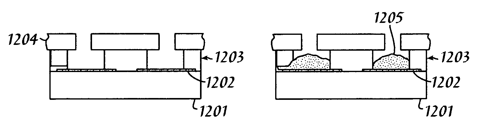
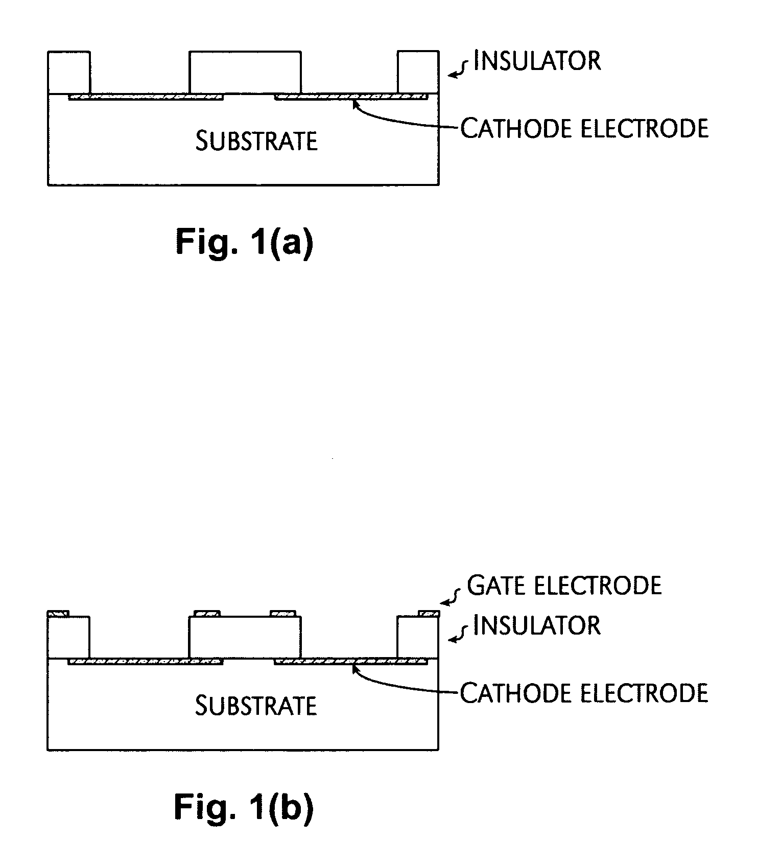
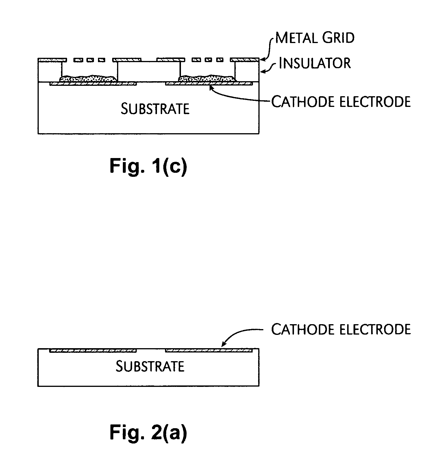
[0027]An embodiment of the present invention provides a process for uniformly depositing CNTs into well structures as shown in FIG. 1(a). Well structures may have four or more walls to form a hole (or one wall if a round hole). The well structure may also be employed as gated, triode structures in which the grid electrodes are deposited on the top of an insulator in advance of CNT deposition (as shown in FIG. 1(b)), or a metal grid is mounted on after CNT deposition in the wells (as shown in FIG. 1(c)). The metal grid can be used to modulate the current from the CNT material ...


PUM

PropertyMeasurementUnit
thickaaaaaaaaaa
thickaaaaaaaaaa
viscosityaaaaaaaaaa

Abstract

Composition of carbon nanotubes (CNTs) are produced into inks that are dispensable via printing or stencil printing processes. The CNT ink is dispensed into wells formed in a cathode structure through a stencil.

Description

[0001]This patent application is a continuation-in-part of U.S. patent application Ser. No. 10 / 937,437, filed Sep. 9, 2004, which claims priority to U.S. Provisional Patent Application Ser. No. 60 / 502,454 filed Sep. 12, 2003.TECHNICAL FIELD[0002]The present invention relates in general to depositing carbon nanotubes with CNT inks into well structures.BACKGROUND INFORMATION[0003]Cathode uniformity is a critical factor for commercializing field emission displays (FEDs). Carbon nanotube (CNT) materials have the highest potential as cathode materials for future FEDs. Uniformly and selectively depositing CNTs over a large substrate is one of the main issues for an FED fabrication process. A typical means of growing carbon nanotubes on a substrate is to use chemical vapor deposition (CVD) techniques with catalyst activation. This technique requires a relatively high growth temperature, thereby increasing the production cost. It is also difficult to achieve a film with uniform properties o...

Claims


Application Information

Patent Timeline
Patent Type & Authority Patents(United States)
IPC IPC(8): H01L51/00H01J19/02H01J19/24
CPCB82Y10/00H01J9/025H01J2201/30469Y10S977/857Y10S977/939Y10S977/72Y10S977/858B82Y40/00H01J1/304
Inventor LI, YUNJUNFINK, RICHARDYANG, MOHSHIYANIV, ZVI
Owner SAMSUNG ELECTRONICS CO LTD
Why Eureka
Try Eureka