

Wafer scale packaging scheme
a packaging scheme and scale technology, applied in the direction of semiconductor devices, semiconductor/solid-state device details, electrical devices, etc., can solve the problems of not necessarily adding value to the latter, and the cost per gate continues to drop year by year
- Summary
- Abstract
- Description
- Claims
- Application Information
AI Technical Summary
Benefits of technology
Problems solved by technology
Method used
Image

Examples
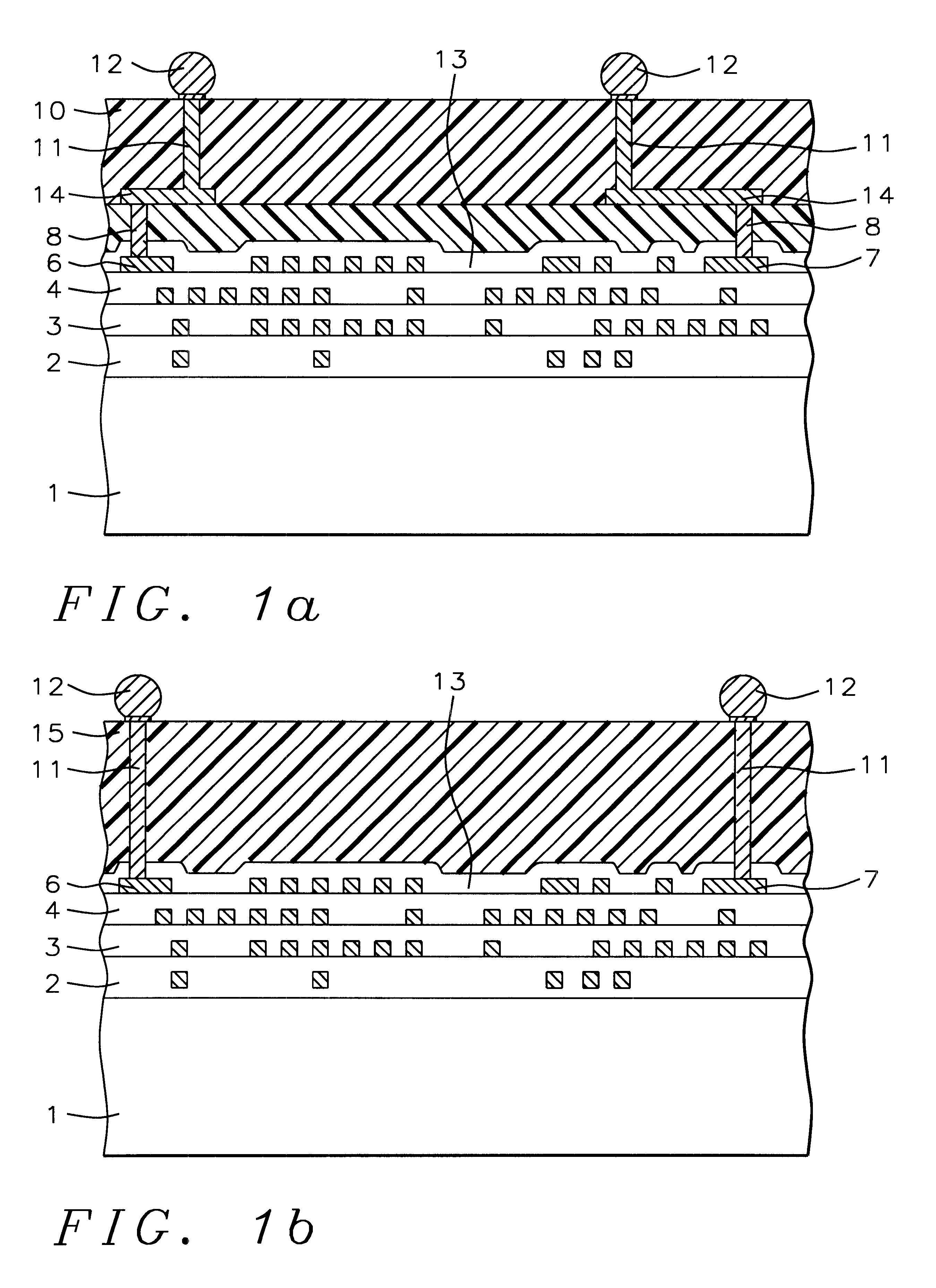
first embodiment
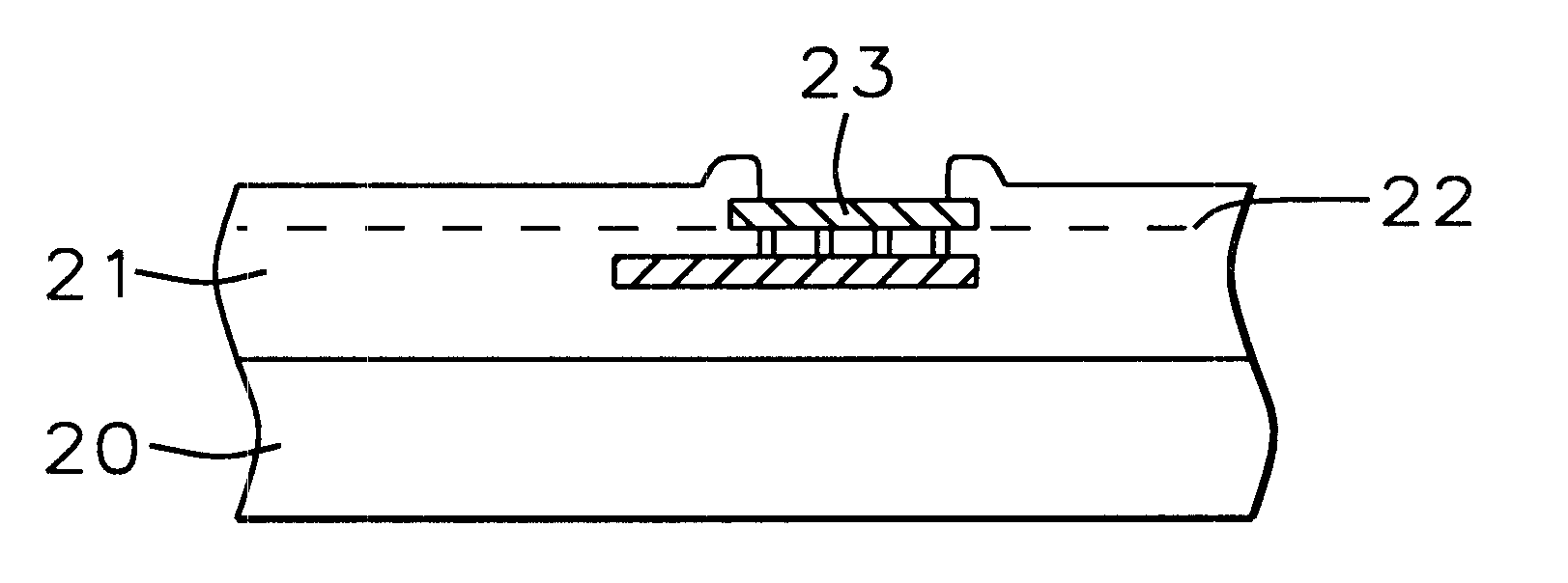
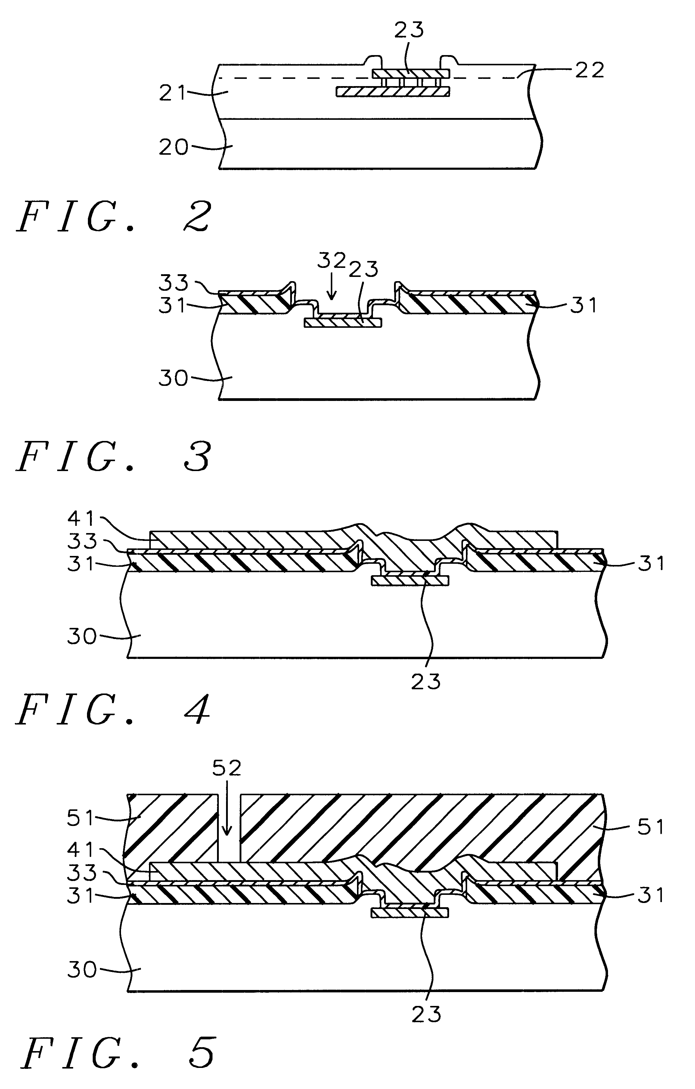
In FIG. 3, layer 30 represents everything in FIG. 2 below the pad 23, including layer 22. Layer 31 of polyimide has been deposited by spin coating onto the surface of 30 and opening 32 has been formed in it using standard photolithographic techniques, including photosensitive polyimides. Layer 31 is generally between about 3 and 20 microns thick. This is followed by the deposition of layer 33 of chrome-copper generally but not necessarily, by sputtering, to a thickness that is between about 500 and 2,000 Angstroms.
With layer 33 (in FIG. 3) covering the entire surface of the wafer, photoresist is laid down and patterned so that the surface is covered everywhere except where it is intended to have the redistribution network. In an important feature of the invention, the individual chip-level distribution networks are connected to one another by using the otherwise empty space provided by the kerf, thereby forming a common distribution network as illustrated in FIG. 12 where individual...
second embodiment
Unlike the first embodiment, there is no redistribution network present on the surface of the unpackaged chips. Therefore, the process proceeds directly from the structure of FIG. 2 to the step of laying down a layer of polymeric material 80 (as illustrated in FIG. 8) whose thickness is between about 20 and 250 microns. As in the first embodiment, via holes 82 are formed in it with the added constraint that they are located directly above studs 23. These correspond to the via holes that will contain conductive posts 11 in FIG. 1b. In order to form these via holes, one of three subprocesses were used: (a) the polymeric material is photosensitive. In the case of polyimides or BCB, there are many commercial compositions available for this. Via holes 52 are then formed by exposing through a suitable mask and developing. By controlling the type of photosensitive material as well as the exposure conditions, the shape of the via holes can be controlled. For example, if the photosensitive m...
third embodiment
As in the second embodiment, there is no redistribution network present on the surface of the unpackaged chips. However, unlike the second embodiment, the preferred metal deposition method is electroplating. Accordingly, a contacting metal layer is deposited over the entire passivation layer. See layer 45 in FIG. 13. This is followed by coating with a layer a photoresist in which via holes are formed in a similar manner to the formation of via holes in the photosensitive versions of the polymers as described in the first and second embodiments, including techniques for controlling the shapes of these via holes. The via holes are then filled with metal by means of electroplating following which the photoresist is stripped, leaving behind freestanding metal posts such as 46 in FIG. 13.
Then, using a differential etch, the contacting layer is removed without any attack on the freestanding posts. Next, the polymeric material is applied to the wafer as a single layer whose thickness is le...
PUM
 Abstract
Description
Claims
Application Information