Power module manufacturing method for connecting nano-silver soldering paste with bare DBC

A power module and nano-silver technology, which is applied in the manufacture of semiconductor/solid-state devices, electrical components, electric solid-state devices, etc. Wetting the substrate, affecting the reliability of chip connection, etc., to achieve the effect of improving connection strength and reliability, low elastic modulus, and high reliability

Active Publication Date: 2018-04-03
TIANJIN UNIV
View PDF4 Cites 10 Cited by
  • Summary
  • Abstract
  • Description
  • Claims
  • Application Information

AI Technical Summary

Problems solved by technology

Traditional nano-silver solder paste connections use silver-plated copper-clad ceramic substrates. However, for nano-silver connections to bare copper substrates or copper-clad substrates, since bare copper substrates or copper-clad substrates are easily oxidized in air, An oxide layer is formed on the surface, so that the nano-silver cannot wet the substrate well, resulting in serious voids and delamination of th...

Method used


Image

  • Power module manufacturing method for connecting nano-silver soldering paste with bare DBC
  • Power module manufacturing method for connecting nano-silver soldering paste with bare DBC
  • Power module manufacturing method for connecting nano-silver soldering paste with bare DBC

Examples


Embodiment 1

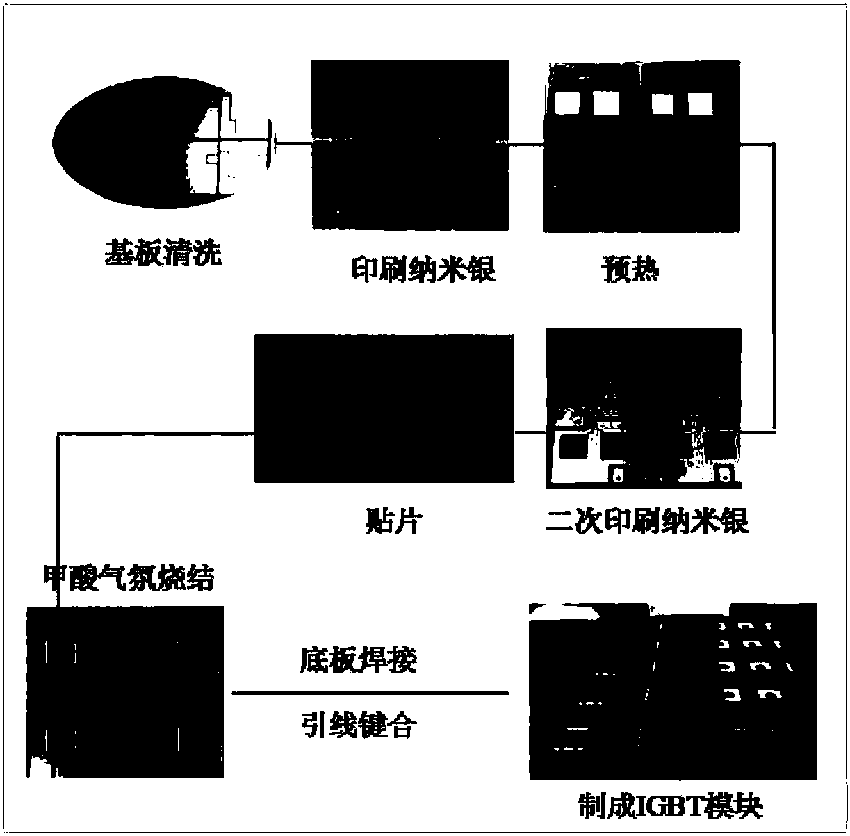
[0031] (1) if figure 1 Shown is the manufacturing process of a high-power semiconductor power module with nano-silver solder paste connected to a bare copper DBC substrate, which are DBC substrate cleaning, nano-silver printing, chip mounting, and nano-silver sintering.

[0032] (2) Cleaning process: first clean the bare copper DBC with dilute hydrochloric acid, and then use an ultrasonic cleaner to vibrate and clean for 1 min, then clean it with absolute ethanol, and use an ultrasonic cleaner to vibrate and clean for 10 min.

[0033] (3) Solder paste printing process, printing nano-silver on the cleaned bare copper DBC, using stencil printing technology to print nano-silver solder paste, preheating after the first printing, preheating temperature 150 ℃, holding time 20min, and then Make a second print.

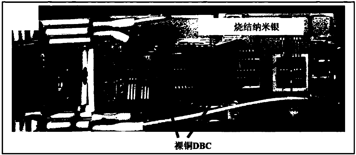
[0034] (4) Mounting process, using a placement machine for placement, the placement pressure is 200gf. See attached Figure 4 ;

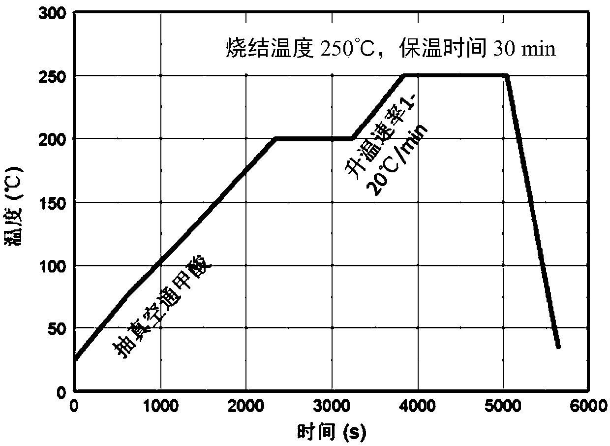
[0035] (5) Sintering process, vacuumize ...

Embodiment 2

[0038] (1) if figure 1 Shown is the manufacturing process of a high-power semiconductor power module with nano-silver solder paste connected to a bare copper DBC substrate, which are DBC substrate cleaning, nano-silver printing, chip mounting, and nano-silver sintering.

[0039] (2) Cleaning process: first clean the bare copper DBC with dilute hydrochloric acid, and then use an ultrasonic cleaner to vibrate and clean for 1 min, then clean it with absolute ethanol, and use an ultrasonic cleaner to vibrate and clean for 10 min.

[0040] (3) Solder paste printing process, printing nano-silver on the cleaned bare copper DBC, printing nano-silver solder paste with stencil printing technology, preheating after the first printing, preheating temperature 180 ℃, holding time 20min, and then Make a second print.

[0041] (4) Mounting process, using a placement machine for placement, the placement pressure is 200gf. See attached Figure 4 ;

[0042] (5) Sintering process, vacuumize t...

Embodiment 3

[0045] (1) if figure 1 Shown is the manufacturing process of a high-power semiconductor power module with nano-silver solder paste connected to a bare copper DBC substrate, which are DBC substrate cleaning, nano-silver printing, chip mounting, and nano-silver sintering.

[0046] (2) Cleaning process: first clean the bare copper DBC with dilute hydrochloric acid, and then use an ultrasonic cleaner to vibrate and clean for 1 min, then clean it with absolute ethanol, and use an ultrasonic cleaner to vibrate and clean for 10 min.

[0047] (3) Solder paste printing process, printing nano-silver on the cleaned bare copper DBC, using stencil printing technology to print nano-silver solder paste, preheating after the first printing, preheating temperature 200 ℃, holding time 20min, and then Make a second print.

[0048] (4) Mounting process, using a placement machine for placement, the placement pressure is 200gf. See attached Figure 4 ;

[0049] (5) Sintering process, vacuumize ...


PUM


Abstract

The invention relates to a power module manufacturing method for connecting nano-silver soldering paste with bare DBC (Direct Bonding Copper). The method comprises a cleaning process, a soldering paste printing process, a chip mounting process and a sintering process. In the cleaning process, the bare DBC is cleaned by adopting ultrasonic oscillation. In the soldering paste printing process, the nano-silver soldering paste is printed by adopting metal stencil printing, and nano-silver is printed twice. In the chip mounting process, chip mounting is performed by adopting a chip mounter. In thesintering process, sintering is performed by adopting a vacuum reflow furnace to obtain an oxygen-free atmosphere of formic acid, and a sintering temperature and a heating rate are controlled. The dense connection between the nano-silver soldering paste and the bare DBC can be realized and the bare DBC can be prevented from being oxidized. No special equipment is required; the treatment process isconvenient and easy; the process is simple; a power chip can be connected with a bare copper substrate or a copper-clad substrate through the nano-silver soldering paste; the reliability of subsequent lead bonding is ensured; the reliability of a power module is improved; and the application of the nano-silver soldering paste to the power semiconductor module packaging is greatly facilitated.

Description

technical field [0001] The invention relates to a method for manufacturing a power module for connecting bare copper DBCs with nano-silver solder paste, and belongs to the field of packaging and manufacturing of high-temperature power electronic modules. Background technique [0002] The chip connection materials of traditional power modules use solder alloys, and their melting points are generally lower than 300°C. This solder alloy is prone to creep fatigue failure due to its low melting point and tendency to generate intermetallic compounds, especially in the high temperature application environment of the module. Therefore, traditional solder alloys have become a major bottleneck restricting high-temperature applications of high-power modules. As a promising thermal interface material, nano-silver solder paste has high thermal conductivity (240W / m K), high electrical conductivity (2.6×10 5 Ω·cm -1 ), low Young's modulus (about 9-20GPa), high melting point (961°C), and...

Claims


Application Information

Patent Timeline
IPC IPC(8): H01L21/60
CPCH01L24/01H01L2224/0603H01L2224/48472H01L2224/49111H01L2224/8384H01L2224/83211
Inventor 梅云辉刘文闫海东李欣陆国权
Owner TIANJIN UNIV
Why Eureka
Try Eureka