

Apparatus for manufacturing semiconductor devices, method of manufacturing the semiconductor devices, and semiconductor device manufactured by the apparatus and method
a manufacturing method and semiconductor technology, applied in the direction of metal working apparatus, manufacturing tools, soldering apparatus, etc., can solve the problems of large heat energy (heat history) received by the substrate and the semiconductor chip, dislocation of the semiconductor chip, and increased manufacturing costs, so as to prevent the occurrence of poor connections and suppress the effect of increasing manufacturing costs
- Summary
- Abstract
- Description
- Claims
- Application Information
AI Technical Summary
Benefits of technology
Problems solved by technology
Method used
Image

Examples
first embodiment
[0044]First, a semiconductor device and an apparatus for manufacturing semiconductor devices according to the present invention will be described.
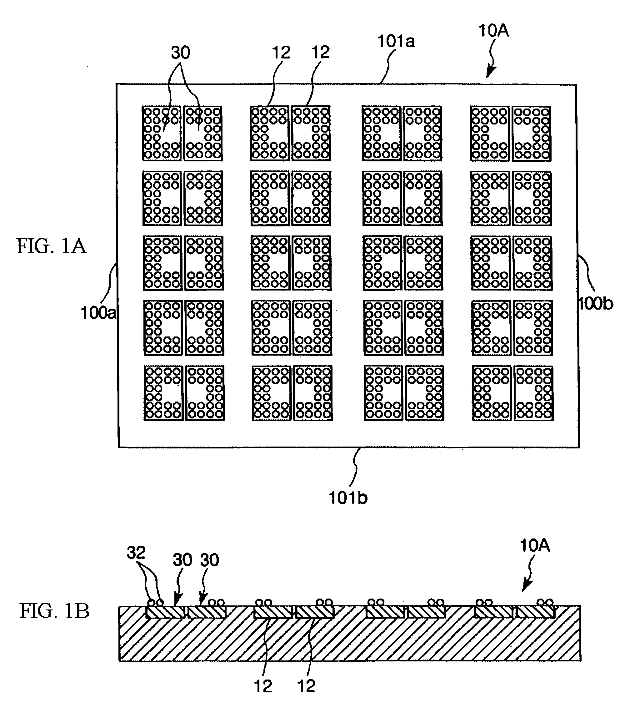
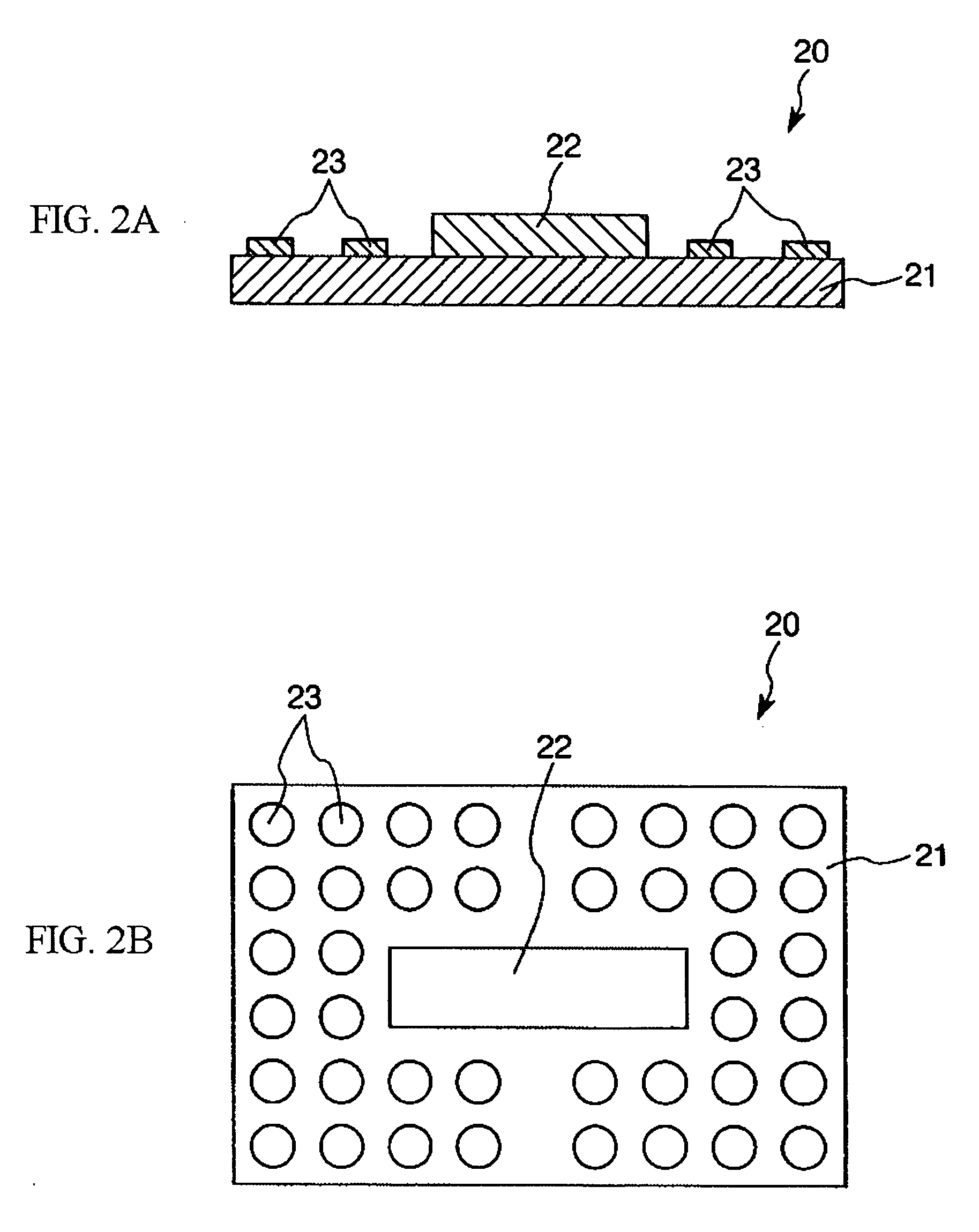
[0045]FIG. 1 is a drawing which shows one example of a structure of an apparatus for manufacturing semiconductor devices according to a first embodiment of the present invention, wherein FIG. 1A is a plan view of the apparatus for manufacturing semiconductor devices, and FIG. 1B is a cross-sectional view of the apparatus for manufacturing semiconductor devices. FIG. 2 is a drawing which shows one example of a structure of a substrate for mounting semiconductor components (lower semiconductor package), wherein FIG. 2A is a cross-sectional view of the substrate for mounting semiconductor components, and FIG. 2B is a plan view of the substrate for mounting semiconductor components. FIG. 3 is a drawing which shows one example of a structure of the semiconductor component (upper semiconductor package), wherein FIG. 3A is a cross-sectional view ...
second embodiment
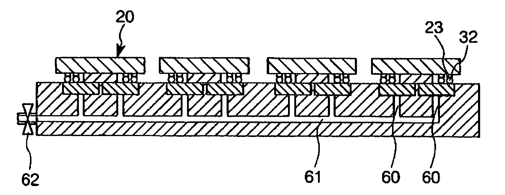
[0082]FIG. 6 is a drawing which shows one example of a structure of an apparatus for manufacturing semiconductor devices according to the present invention, wherein FIG. 6A is a plan view of the apparatus for manufacturing semiconductor devices, and FIG. 6B is a cross-sectional view of the apparatus for manufacturing semiconductor devices. In the description given below, the upper side in FIG. 6B is referred to as “upper”, and the lower side in FIG. 6B is referred to as “lower”.
[0083]First, the structure of an apparatus 10B for manufacturing semiconductor devices of the second embodiment will be described.
[0084]The apparatus 10B for manufacturing semiconductor devices shown in FIG. 6 further has a plurality of decompression holes (part of suction flow path) 60 that open at the bottom portions of the respective receiving portions 12 in comparison with the apparatus 10A for manufacturing semiconductor devices shown in FIG. 1. In the apparatus 10B for manufacturing semiconductor device...
third embodiment
[0101]FIG. 8 is a drawing which shows one example of a structure of an apparatus for manufacturing semiconductor devices according to the present invention, wherein FIG. 8A is a plan view of the apparatus for manufacturing semiconductor devices, and FIG. 8B is a cross-sectional view of the apparatus for manufacturing semiconductor devices. In the description given below, the upper side in FIG. 8B is referred to as “upper”, and the lower side in FIG. 8B is referred to as “lower”.
[0102]An apparatus 10C for manufacturing semiconductor devices shown in FIG. 8 further has a plurality of heatproof adhesive sheets (adhesive material) 80 provided on the bottom portions of the respective receiving portions 12 in comparison with the apparatus 10A for manufacturing semiconductor devices shown in FIG. 1. By providing such heatproof adhesive sheets, it is possible to immovably hold the upper semiconductor packages 30 in the respective receiving portions 12 of the apparatus 10C for manufacturing ...
PUM
| Property | Measurement | Unit |
|---|---|---|
| thickness | aaaaa | aaaaa |
| thickness | aaaaa | aaaaa |
| atmospheric temperature | aaaaa | aaaaa |
Abstract
Description
Claims
Application Information