Supercharge Your Innovation With Domain-Expert AI Agents!

Method for growing epitaxial crystal

a technology of epitaxial crystal and crystal growth, which is applied in the growth process of crystals, polycrystalline materials, chemically reactive gases, etc., can solve the problems of deteriorating production efficiency and inability to obtain desired carrier concentrations, and achieve the effect of improving production efficiency and changing doping efficiency

Active Publication Date: 2008-12-16
JX NIPPON MINING & METALS CORP
View PDF8 Cites 2 Cited by
  • Summary
  • Abstract
  • Description
  • Claims
  • Application Information

AI Technical Summary

Benefits of technology

[0029]According to the present invention, the change in the doping efficiency to the off angle of the substrate can be easily found from the relation between the off angle of the substrate and the doping efficiency which is obtained in advance. Thus, it can be easily predicted how the doping condition, such as the dopant flow rate, should be corrected depending on the off angle of the substrate to be used.
[0030]Therefore, it is not required to carry out the epitaxial growth for every substrate lot to find and set the doping condition for a desired carrier concentration. Thus, the doping condition for growing the epitaxial crystal having a desired carrier concentration can be established by the small number of test runs. As a result, it is possible to remarkably improve the production efficiency.

Problems solved by technology

A problem where a desired carrier concentration could not be obtained even when growth conditions were fixed, was caused.
Therefore, the production efficiency was deteriorated.

Method used


Image

  • Method for growing epitaxial crystal
  • Method for growing epitaxial crystal

Examples


example 1

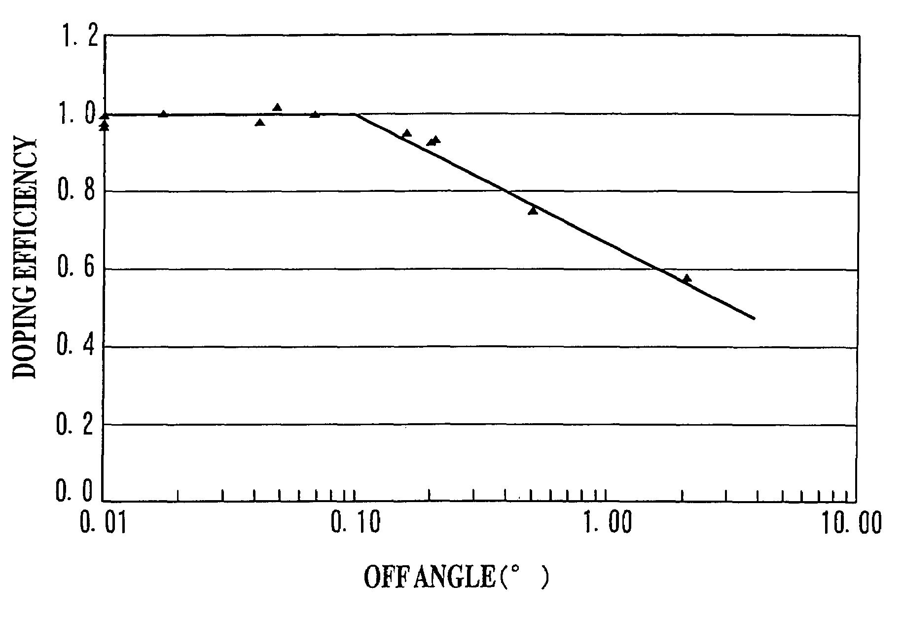
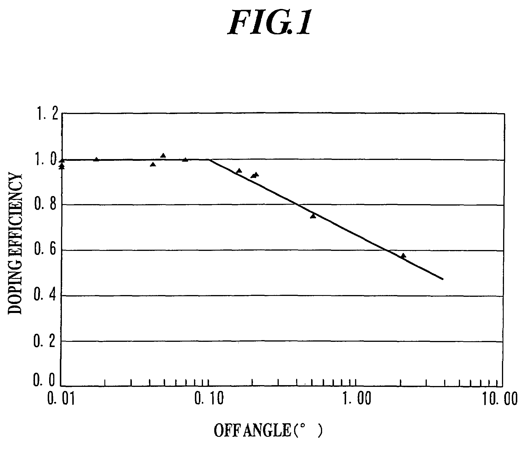
[0041]By using InP substrate having an off angle of 0.15°, a diameter of 2 inches, an S-doped concentration of 4×1018 cm−3, and a thickness of 350 μm, an InP epitaxial crystal layer having a thickness of 1 μm and a target carrier concentration 1.2×1018 cm−3 was formed by the MOCVD method. Then, by considering the decrease of a doping efficiency to an off angle of 0.15° based on FIG. 1, the dopant flow rate was 1.05 times higher than that of the experiment (3). In the obtained epitaxial crystal layer, the haze was 2.5 ppm which is the same result as that of the above experiment (3). However, the carrier concentration was 1.18×1018 cm−3 that is closer to the target value.

example 2

[0042]By using a plurality of InP substrates having an off angle of 0.15±0.03°, a diameter of 2 inches, an S-doped concentration of 4×1018 cm−3, and a thickness of 350 μm, InP epitaxial crystal layers having a thickness of 1 μm and a target carrier concentration 1.2×1018 cm−3 were formed by the MOCVD method. Then, by considering the decrease of a doping efficiency to an off angle of 0.15° based on FIG. 1, the dopant flow rate was 1.05 times higher than that of the experiment (3). In the obtained epitaxial crystal layer, the haze was 2.5 ppm which is the same result as that of the above experiment (3). However, the carrier concentration was 1.17 to 1.22×1018 cm−3 that is closer to the target value. It is noted that in only InP substrates having an off angle of 0.15±0.02°, the carrier concentration was 1.19 to 1.22×1018 cm−3.

example 3

[0043]By using a plurality of InP substrates having an off angle of 0.05 to 0.10°, a diameter of 2 inches, an S-doped concentration of 6×1018 cm−3, and a thickness of 350 μm, InP epitaxial crystal layers having a thickness of 1 μm and a target carrier concentration 4.8×1017 cm−3 were formed by the MOCVD method. Then, because the carrier concentration of an epitaxial crystal layer was 4.8×1017 cm−3 in case of using a substrate having an off angle of 0.05° and in case of the doping flow rate of 47 sccm, the same doping flow rate was set in the present example. In the obtained epitaxial crystal layer, the haze was 1.04 to 1.35 ppm, the carrier concentration was 4.8±0.1×1017 cm×3, and the ratio of the doping efficiency was 1.0. Specifically, as shown in FIG. 1, the correction of doping conditions were not required in a range of an off angle of not more than 0.1°.

[0044]In the present example, for example, in a production run in which a doping condition (dopant flow rate) is previously kn...


PUM

PropertyMeasurementUnit
off angleaaaaaaaaaa
average off angleaaaaaaaaaa
off angleaaaaaaaaaa

Abstract

It is to provide a method for growing an epitaxial crystal in which the doping conditions are set when an epitaxial crystal having a desired carrier concentration is grown. A method for growing an epitaxial crystal while a dopant is added to a compound semiconductor substrate, comprises: obtaining a relation between an off angle and a doping efficiency with regards to the same type of compound semiconductor substrate in advance; and setting a doping condition for carrying out an epitaxial growth on the compound semiconductor substrate based on the obtained relation and a value of the off angle of the subtrate.

Description

TECHNICAL FIELD[0001]The present invention relates to a method for growing epitaxial crystal including a compound semiconductor. In particular, the present invention relates to a technique for easily setting doping conditions for growing epitaxial crystal having a desired carrier concentration.BACKGROUND ART[0002]Conventionally, for the application of a semiconductor element such as a light-emitting element or a light-receiving element, a semiconductor wafer which is obtained by epitaxially growing a III-V system compound semiconductor layer, for example, InP, on an InP substrate, has been widely used. The epitaxial layer of the compound semiconductor is formed, for example, by the metalorganic chemical vapor deposition method (hereinafter referred to as MOCVD method).[0003]When the above-described III-V system compound semiconductor layer is epitaxially grown by the MOCVD method, minute convex defects called hillock and wrinkle defects called orange peel are caused on the surface o...

Claims


Application Information

Patent Timeline
Patent Type & Authority Patents(United States)
IPC IPC(8): C30B25/12
CPCC30B25/16C30B25/20C30B29/40H01L21/02392H01L21/02433H01L21/02543H01L21/02576H01L21/20
Inventor KAWABE, MANABUHIRANO, RYUICHI
Owner JX NIPPON MINING & METALS CORP
Features
  • R&D
  • Intellectual Property
  • Life Sciences
  • Materials
  • Tech Scout
  • Unparalleled Data Quality
  • Higher Quality Content
  • 60% Fewer Hallucinations
Learn More