Photosensitive metal nanoparticle and method of forming conductive pattern using the same

a metal nanoparticle and conductive pattern technology, applied in the field of photosensitive metal nanoparticles and methods of forming conductive patterns using the same, can solve the problems of difficult to prepare metal nanoparticle films or patterns in a large size, difficult to overcome such fine particles, and difficult control and array such fine particles efficiently

Inactive Publication Date: 2009-01-06
SAMSUNG ELECTRONICS CO LTD
View PDF2 Cites 10 Cited by
  • Summary
  • Abstract
  • Description
  • Claims
  • Application Information

AI Technical Summary

Benefits of technology

[0010]The present inventors devoted much effort to satisfying the demand in the prior art and found that when using photosensitive metal nano-particles that are prepared by forming a self-assembled monolayer of thiol (—SH) or isocyanide (—CN) compounds having a terminal reactive group on a surface of the metal nano-particles and introducing a photosensitive group through the reaction with the terminal reactive group to the monolayer, a pattern of the metal nanoparticles can be easily prepared over a large area via photolithography process, without performing sputtering or etching process.

Problems solved by technology

However, for metal nano particles to be used in a form of film or pattern, there remains difficulties to overcome, i.e. controlling and arraying such fine particles efficiently.
However, in the case of using the self-assembled monolayer method, it is not easy to prepare metal nanoparticle films or patterns in a large size because of difficulty in controlling molecular orientation or spatial ordering, instability or aggregation of the metal nanoparticles in a thin film, and defects of film.
For this reason, the metal nano particle or its film or pattern has been limited in their commercial application.

Method used


Image

  • Photosensitive metal nanoparticle and method of forming conductive pattern using the same
  • Photosensitive metal nanoparticle and method of forming conductive pattern using the same
  • Photosensitive metal nanoparticle and method of forming conductive pattern using the same

Examples


example 1

Introduction of Photosensitive group to Surface of Gold Nanoparticles

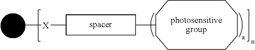
[0060]0.2 g of the gold nanoparticles prepared in Preparative Example 1 was dispersed in 5 g of cystamine dihydrochloride, and stirred by use of a magnetic bar for 2 hours, filtered, and then washed with pure water and filtered, to obtain gold nanoparticles each having a surface substituted with amine groups. While the pH being maintained at 7.2-7.4 in a buffer solution of 0.05 M 4-(2-hydroxyethyl)-1-piperrazineethanesulfonic acid (HEPES), the gold nanoparticles were reacted with acrylic acid (0.01 M) for 4 hours, in the presence of 1-ethyl-3(3-dimethylaminopropyl)carbodiimide (EDC) as a condensation reaction agent. After the completion of the reaction, resulting metal nanoparticles were filtered, washed twice with THF, and dried under a reduced pressure, to yield photosensitive metal nanoparticles having acryl moieties connected through an amide group on the surface thereof.

example 2

Introduction of Photosensitive group to Surface of Silver Nanoparticles

[0061]Silver nanoparticles having acryl moieties connected through an amide group on the surface thereof were obtained in the same manner as in Example 1, with the exception that 0.2 g of the silver nanoparticles prepared in Preparative Example 2 was used, instead of the gold nanoparticles.

example 3

Introduction of Photosensitive group to Surface of Copper Nanoparticles

[0062]Copper nanoparticles having acryl moieties connected through an amide group on the surface thereof were obtained in the same manner as in Example 1, with the exception that 0.2 g of the copper nanoparticles prepared in Preparative Example 3 was used, instead of the gold nanoparticles.


PUM

PropertyMeasurementUnit
particle sizeaaaaaaaaaa
sizeaaaaaaaaaa
sizeaaaaaaaaaa

Abstract

A photosensitive metal nanoparticle and a method of forming a conductive pattern using the same, wherein a self-assembled monolayer of a thiol compound or isocyanide compound having a terminal reactive group is formed on a surface of the metal nanoparticle and a photosensitive group is introduced to the terminal reactive group. The photosensitive metal nanoparticles can easily form a conductive film or pattern having excellent conductivity upon exposure to UV, and thus can be applied for antistatic washable sticky mats or shoes, conductive polyurethane printer rollers, electromagnetic interference shielding, etc.

Description

[0001]This non-provisional application is a continuation application of application Ser. No. 10 / 734,138 filed on Dec. 15, 2003 and claims priority under 35 U.S.C. § 119(a) from Korean Patent Application No. 2003-37040 filed on Jun. 10, 2003, which is herein incorporated by reference.BACKGROUND OF THE INVENTION[0002]1. Field of the Invention[0003]The present invention relates, generally, to photosensitive metal nanoparticles and methods of forming conductive patterns using the same. More specifically, the present invention relates to a photosenstivie metal nanoparticle, produced by forming a self-assembled monolayer of a thiol or isocyanide compound having a terminal reactive group on its surface and introducing a photosensitive group through the terminal reactive group; and a method of forming a conductive pattern using the same.[0004]2. Description of the Related Art[0005]Nano-sized materials, having various electrical, optical and biological properties depending on the orders and ...

Claims


Application Information

Patent Timeline
Patent Type & Authority Patents(United States)
IPC IPC(8): G03C1/52G03C1/735G03F7/027B82B3/00G03F7/004G03F7/016G03F7/16
CPCG03F7/0047G03F7/027G03F7/165B82Y30/00B82Y40/00G03F7/016Y10S430/117B82B3/00
Inventor PARK, JONG JINJEONG, EUN JEONGLEE, SANG YOON
Owner SAMSUNG ELECTRONICS CO LTD
Why Eureka
Try Eureka