Methods for forming shielded gate field effect transistors

a gate field effect transistor and gate field effect technology, applied in the direction of basic electric elements, semiconductor devices, electrical equipment, etc., can solve the problems of low on-state power loss, high power conversion efficiency, and high electric field

Active Publication Date: 2009-01-13
SEMICON COMPONENTS IND LLC
View PDF9 Cites 71 Cited by
  • Summary
  • Abstract
  • Description
  • Claims
  • Application Information

AI Technical Summary

Problems solved by technology

Improving these and other characteristics results in very low on-state power losses and switching losses in turn resulting in high power conversion efficiencies in applications such as DC-DC converters.
One problem with the shielded gate trench MOSFET shown in FIG. 1 is that gate electrode 118 typically has sharp bottom corners which with the flat top surface of shield electrode 114 leads to high electric fields in these regions.
If the IED dielectric layer is too thin, gate to source shorts may occur.
If the dielectric is too thick, it may be difficult to align the diffused body region with the top surface of the IED region to ensure that the gate electrode extends below the bottom surface of the body region.
Another drawback of conventional power FETs is that the drift region represents up to 40% of the total RDSon, significantly limiting improvements in RDSon.
However, reducing the cell pitch is limited by manufacturing and design limitations, such as the minimum critical dimensions of photolithography tools and misalignment tolerances.
A parasitic BJT could be turned on at a very low current, resulting in a poor SOA and lower UIS capability.

Method used


Image

  • Methods for forming shielded gate field effect transistors
  • Methods for forming shielded gate field effect transistors
  • Methods for forming shielded gate field effect transistors

Examples


Embodiment Construction

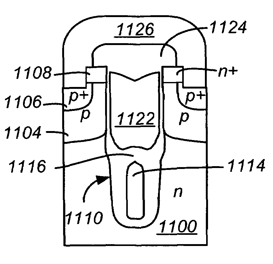
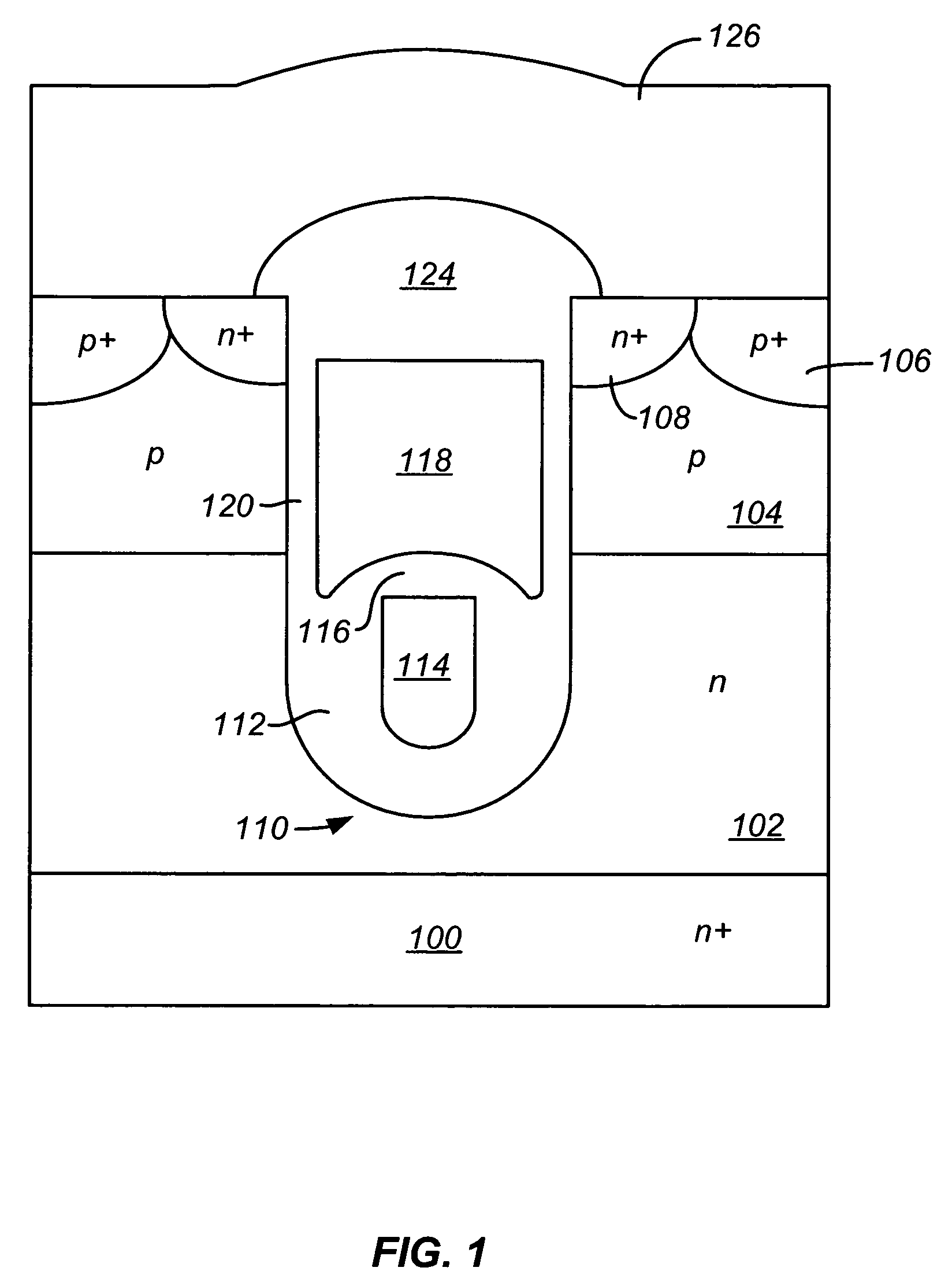
[0030]In accordance with embodiments of the present invention, structures and methods for forming a shielded gate trench FET with an improved IED layer are disclosed. Also disclosed are structures and methods for forming shielded gate trench FETs with an improved IED layer and self aligned regions that allow the cell pitch to be reduced without increasing the process complexity. The various embodiments of the invention will be described in further detail below.

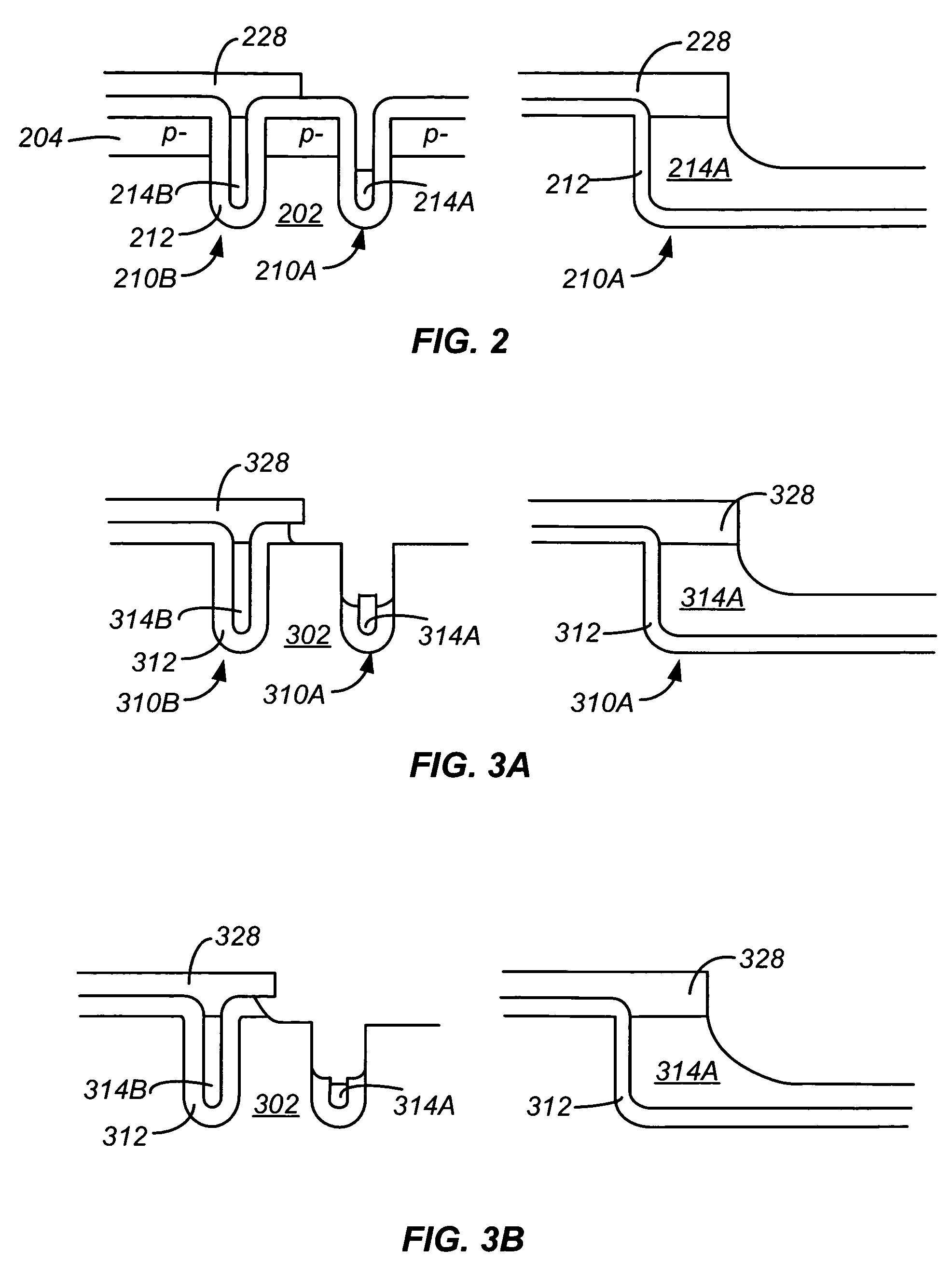
[0031]FIG. 2 shows two side-by-side cross sectional views corresponding to an intermediate process step for forming a shielded gate trench FET in accordance with a first embodiment of the present invention. The left diagram of FIG. 2 corresponds to a cross sectional view in the active region of the FET. The right diagram corresponds to a cross sectional view along the dimension perpendicular to the page and through the right trench in the left diagram, showing the termination of the right trench at the edge of the active regio...


PUM


Abstract

A field effect transistor is formed as follows. A trench is formed in a semiconductor region. A dielectric layer lining the trench sidewalls and bottom is formed. The trench is filled with a conductive material. The conductive material is recessed into the trench to thereby form a shield electrode in a bottom portion of the trench. The recessing of the conductive material includes isotropic etching of the conductive material. An inter-electrode dielectric (IED) is formed over the recessed shield electrode.

Description

CROSS-REFERENCES TO RELATED APPLICATIONS[0001]This application claims the benefit of U.S. Provisional Application No. 60 / 695,718, filed Jun. 29, 2005, which is incorporated herein by reference in its entirety for all purposes.BACKGROUND OF THE INVENTION[0002]The present invention relates to semiconductor power field effect transistors (FETs), and more particularly to structures and methods for forming improved shielded gate FETs.[0003]Shielded gate trench FETs are advantageous over conventional field effect transistor devices in that the shield electrode reduces the gate-drain capacitance (Cgd) and improves the breakdown voltage of the transistor. However, further improvements can be made. There is a need for power FETs with improved performance including lower on-resistance (RDSon), higher blocking voltage, and lower gate charges. Sufficient ruggedness is also important, since the ruggedness defines the safe operating area (SOA) and the unclamped inductive switching (UIS) of the de...

Claims


Application Information

Patent Timeline
Patent Type & Authority Patents(United States)
IPC IPC(8): H01L21/336H01L21/4763
CPCH01L29/407H01L29/66719H01L29/66727H01L29/66734H01L29/7811H01L29/7813H01L21/26586H01L29/0865H01L29/0869H01L29/41766H01L29/4236H01L29/42368H01L29/42376H01L21/18
Inventor GREBS, THOMAS E.KRAFT, NATHAN LAWRENCERIDLEY, RODNEY
Owner SEMICON COMPONENTS IND LLC
Why Eureka
Try Eureka