Method for forming high-K charge storage device

a memory device and high-k charge technology, applied in semiconductor/solid-state device manufacturing, basic electric elements, electric devices, etc., can solve the problems of scaling and scaling issue, and achieve the effect of reducing repetition

Active Publication Date: 2009-01-20
CHARTERED SEMICONDUCTOR MANUFACTURING
View PDF17 Cites 40 Cited by
  • Summary
  • Abstract
  • Description
  • Claims
  • Application Information

AI Technical Summary

Problems solved by technology

A key issue for floating-gate nonvolatile semiconductor memories (NVMs) is the scaling of the tunneling oxide because the stress-induced leakage current (SILC) limits the tunnel oxide to ˜8 nm.
This scaling issue is a formidable challenge especially for the emerging system-on-chip (SOC) integrated circuits designs in which programming voltage must be scaled for the NVMs to be compatible with the low voltage logic circuits.
However, retention and erase speed remain as the major challenges for conventional SONOS devices as device and voltage further scale in the future.

Method used


Image

  • Method for forming high-K charge storage device
  • Method for forming high-K charge storage device
  • Method for forming high-K charge storage device

Examples


first example embodiment

II. First Example Embodiment

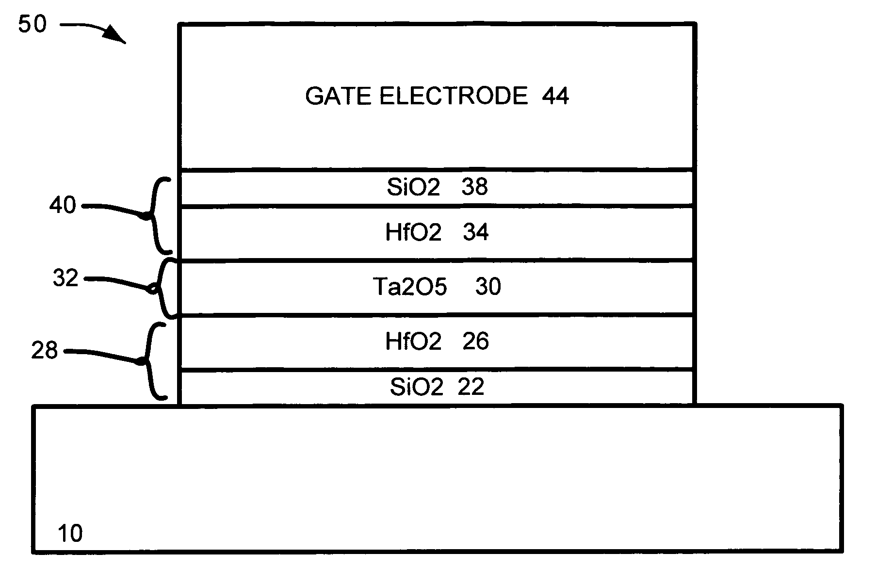
[0057]The first example embodiment of a memory structure is depicted in FIG. 1. It preferably employs a top blocking layer 40 comprised of SiO2 / HfO2 3834, a charge storage layer 32 comprised of Ta2O5, and a bottom tunnel dielectric 28 comprised of HfO2 / SiO2 2622. The top and bottom SiO2 3822 are preferably very thin, 2 layers serves to improve the retention and interfacial quality for the bottom Si and gate electrode. The HfO2 layers can improve the erase speed as compared to a conventional SONOS. The top HfO2 layer 34 thickness preferably ranges from 5 to 20 nm, while the bottom HfO2 layer 26 thickness preferably ranges from 1 to 6 nm. The Ta2O5 layer 30 preferably thickness ranges from 3 to 8 nm. Using high-k materials allow further device and voltage scaling. They can be deposited using CVD or PVD processes. The gate electrode 44 can be metal or polysilicon.

[0058]A first example embodiment for a method of fabrication of a floating gate non-volatile mem...

second example embodiment

III. Second Example Embodiment

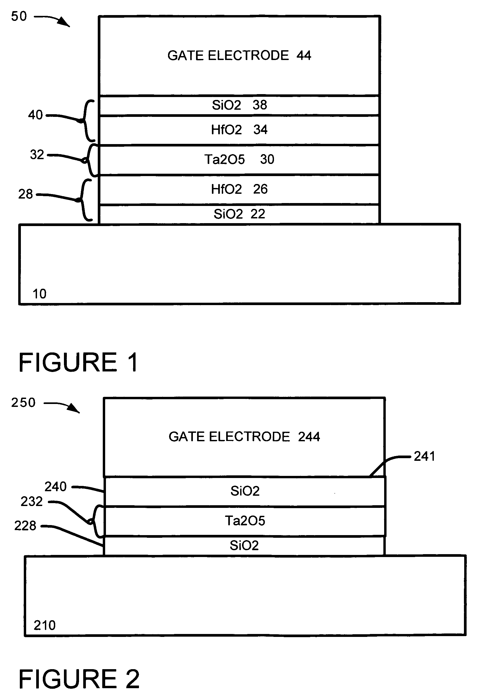
[0087]A second example embodiment is shown in FIG. 2 and the flowchart in FIG. 4. Corresponding layers and process can be carried out as described above in the first example embodiment.

[0088]The second example embodiment of a memory structure is depicted in FIG. 2. It preferably employs a top blocking layer 240 comprised of SiO2, a charge storage layer 232 comprised of Ta2O5, and a bottom tunnel dielectric 228 comprised of SiO2. The gate electrode 244 can be metal or polysilicon.

A. A Bottom Tunnel Layer

[0089]We provide a substrate. We form a bottom tunnel layer 228 over a substrate 210.

[0090]The bottom tunnel layer 228 is preferably comprised essentially of silicon oxide and has a thickness between 1 and 4 nm and more preferably about 2 nm.

B. Bottom Layer Anneal Step

[0091]Referring to FIG. 4, step 204, in an optional tunnel nitridation step, annealing the bottom tunnel layer 28 in a nitrogen and hydrogen containing atmosphere.

[0092]The tunnel anneal ste...


PUM


Abstract

Structures and methods of fabricating of a floating gate non-volatile memory device. In a first example embodiment, We form a bottom tunnel layer comprised of a lower oxide tunnel layer and a upper hafnium oxide tunnel layer; a charge storage layer comprised of a tantalum oxide and a top blocking layer preferably comprised of a lower hafnium oxide storage layer and an upper oxide storage layer. We form a gate electrode over the top blocking layer. We pattern the layers to form a gate structure and form source / drain regions to complete the memory device. In a second example embodiment, we form a floating gate non-volatile memory device comprised of: a bottom tunnel layer comprised essentially of silicon oxide; a charge storage layer comprised of a tantalum oxide; a top blocking layer comprised essentially of silicon oxide; and a gate electrode. The embodiments also comprise anneals and nitridation steps.

Description

BACKGROUND OF INVENTION[0001]1) Field of the Invention[0002]This invention relates generally to the structure and fabrication of semiconductor devices and more particularly to the fabrication of a dielectric materials for memory devices.[0003]2) Description of the Prior Art[0004]A key issue for floating-gate nonvolatile semiconductor memories (NVMs) is the scaling of the tunneling oxide because the stress-induced leakage current (SILC) limits the tunnel oxide to ˜8 nm. This scaling issue is a formidable challenge especially for the emerging system-on-chip (SOC) integrated circuits designs in which programming voltage must be scaled for the NVMs to be compatible with the low voltage logic circuits. Therefore, silicon-oxide-nitride-oxide-silicon (SONOS) charge-trapping based NVM is replacing floating-gate NVM due to its advantages of lower programming voltage, smaller cell size and better endurance over the floating-gate devices. However, retention and erase speed remain as the major ...

Claims


Application Information

Patent Timeline
Patent Type & Authority Patents(United States)
IPC IPC(8): H01L21/76
CPCH01L21/28282H01L29/513H01L29/792H01L29/40117
Inventor ANG, CHEW HOESOHN, DONG KYUNHSIA, LIANG CHOO
Owner CHARTERED SEMICONDUCTOR MANUFACTURING
Why Eureka
Try Eureka