Method for analyzing the reliability of optoelectronic elements rapidly

a technology of optoelectronic elements and reliability analysis, applied in the field of rapid analysis of can solve the problems of destroying the elements, taking a long time for the current reliability analysis of optoelectronic elements, and ineffective mass production shipping, etc., to achieve rapid analysis of reliability and analyze the reliability of optoelectronic elements.

Inactive Publication Date: 2009-01-20
SOUTHERN TAIWAN UNIVERSITY OF TECHNOLOGY
View PDF3 Cites 2 Cited by
  • Summary
  • Abstract
  • Description
  • Claims
  • Application Information

AI Technical Summary

Benefits of technology

[0009]The present invention relates to a method for analyzing the reliability of optoelectronic elements rapidly. In the present invention, the sampling optoelectronic elements are imposed with the appropriate forward bias and reverse bias to generate alternate cycles of positive currents and negative currents. Then, the optoelectronic elements are proceeded with appropriate iteration cycles, cycle time and duty cycles. Next, the spectrum analyzer tests and measures the optoelectronic elements which have been proceeded with the electrical cycle test to determine whether the NEP and peak of noise power spectrum of the optoelectronic elements at the low frequency with the electrical cycle test are increased. The NEP and peak of noise power spectrum of the optoelectronic elements at the low frequency after the electrical cycle test are compared with the statistic standard deviation to find out the optoelectronic elements that have reliability problems, and to achieve rapid analysis of the reliability.

Problems solved by technology

However, the current methods for the reliability analysis of the diode chips need to take couple days and the process is very complicated, thereby easily resulting in ineffective shipping for mass production.
1. It takes very long time for the current reliability analysis of the optoelectronic elements.
2. The current reliability analysis of the optoelectronic elements will be destructive to the elements.

Method used


Image

  • Method for analyzing the reliability of optoelectronic elements rapidly
  • Method for analyzing the reliability of optoelectronic elements rapidly
  • Method for analyzing the reliability of optoelectronic elements rapidly

Examples


Embodiment Construction

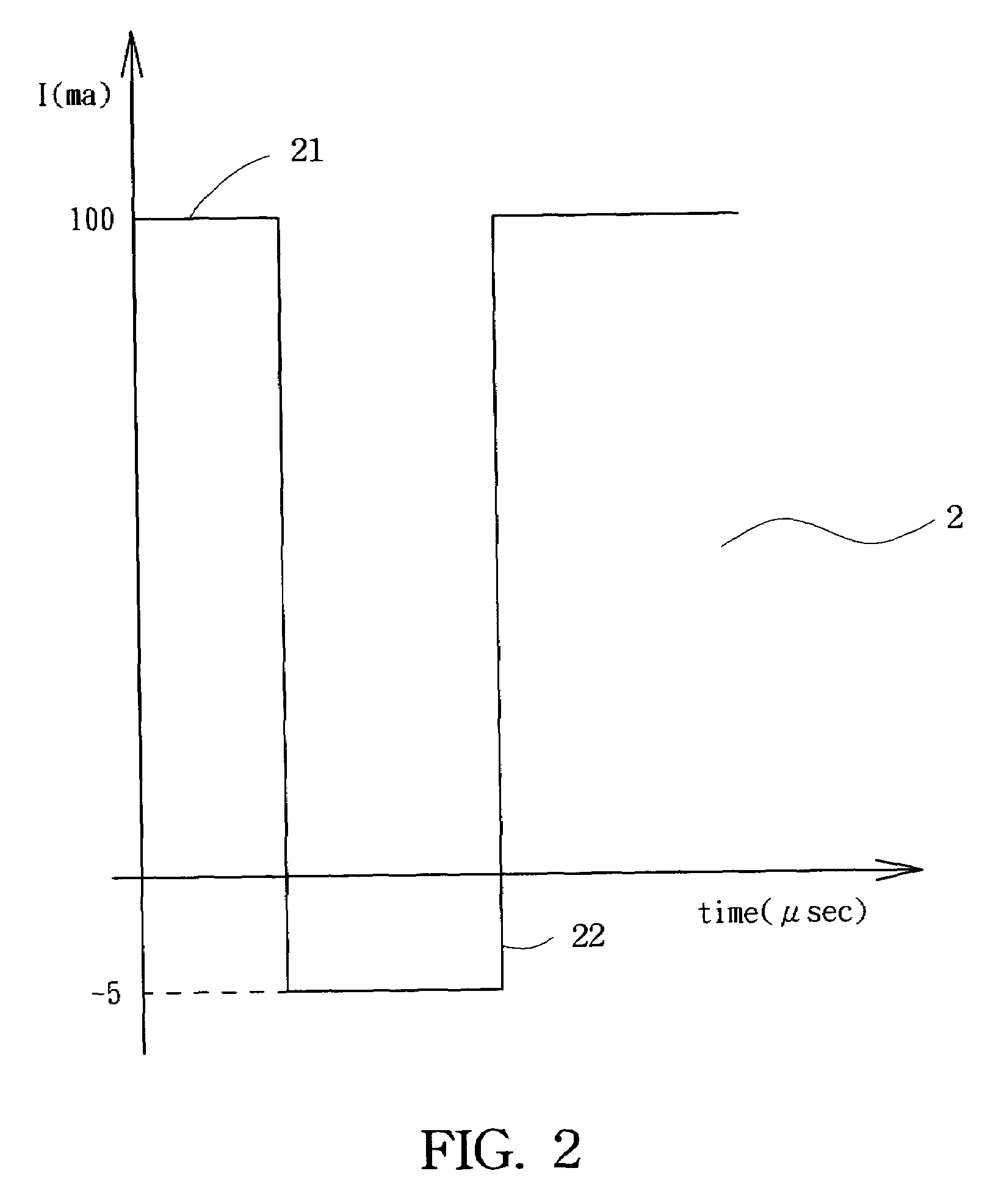
[0013]The foregoing aspects and many of the attendant advantages of this invention are more readily appreciated as the same become better understood by reference to the following detailed description, when taken in conjunction with the accompanying drawings.

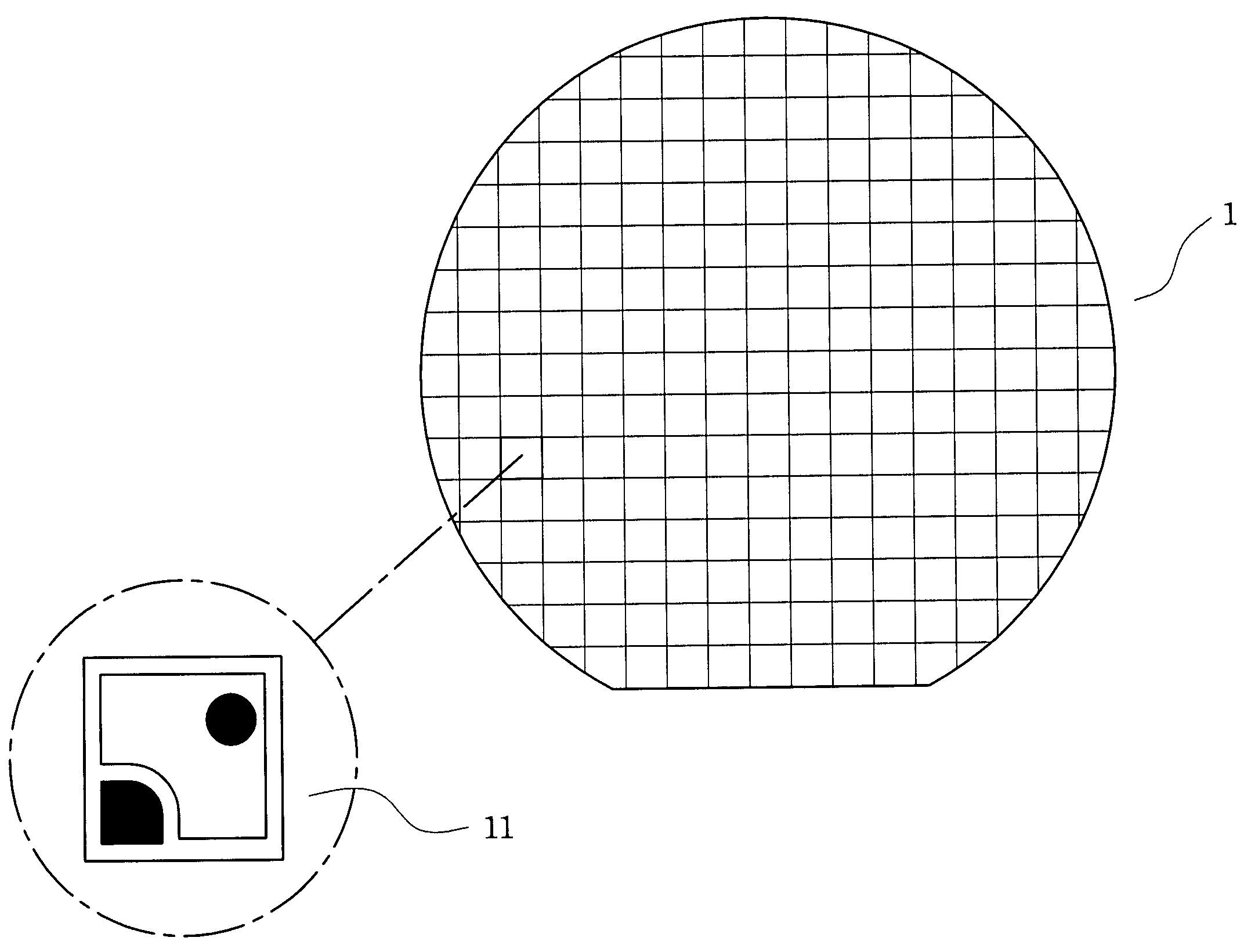
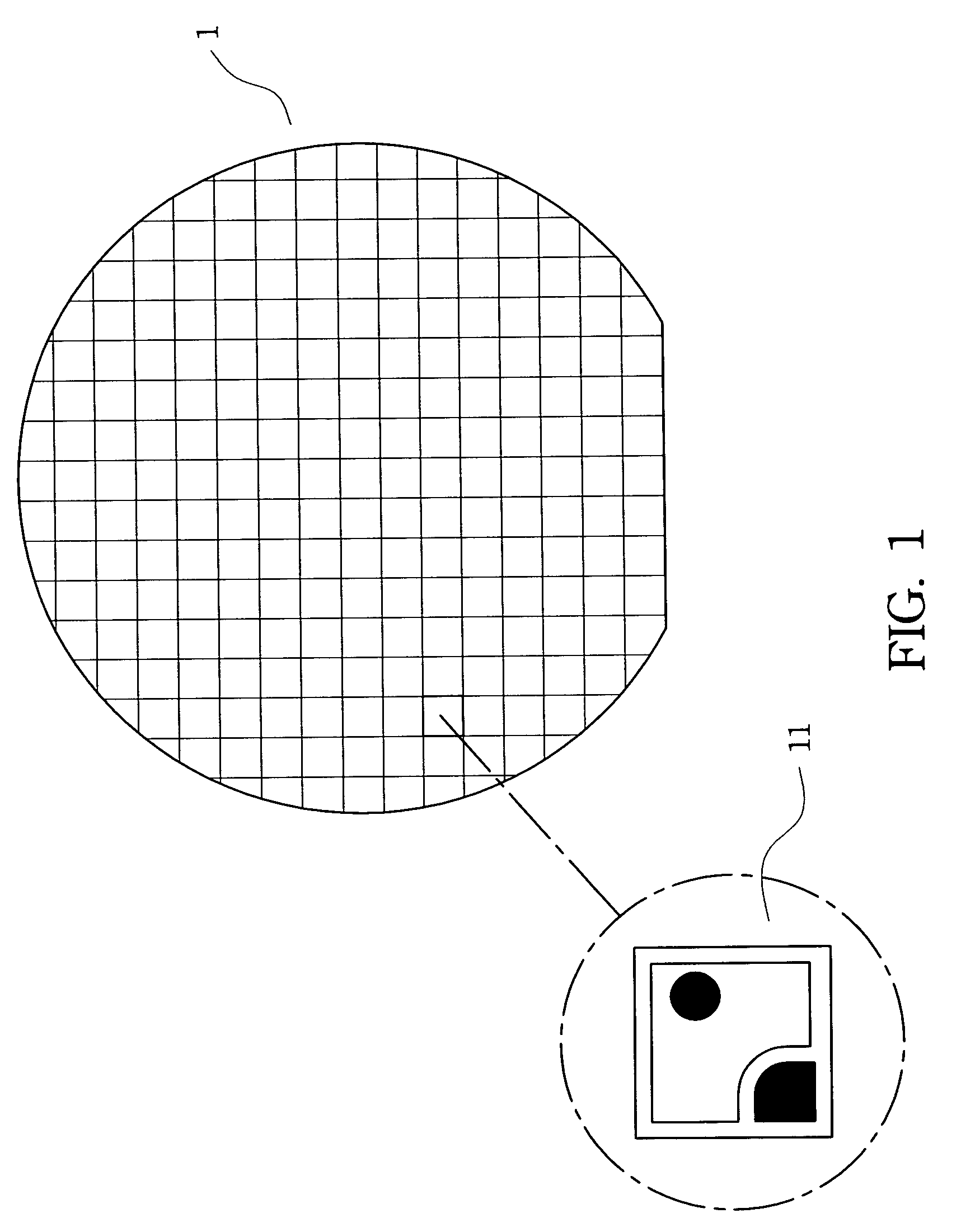
[0014]Refer to FIG. 1 and FIG. 2. In the method used for analyzing the reliability of optoelectronic elements rapidly of the present invention, one hundred optoelectronic elements 11 which are good elements determined by the electrical probing test are taken out from a wafer 1 to be testing pieces for rapid reliability analysis. Each optoelectronic element 11 is 300 μm in length and 300 μm in width. A spectrum analyzer is used to test and measure NEP and peak of noise power spectrum of the optoelectronic elements 11 at a low frequency, wherein the NEP, the peak of noise power spectrum, and the multiplication product of the NEP and the peak of noise power spectrum of each optoelectronic element respectively respect three standard ...


PUM


Abstract

A method for analyzing the reliability of optoelectronic elements rapidly is described. A plurality of optoelectronic elements are tested and measured by a spectrum analyzer to obtain noise equivalent power (NEP) and peak of noise power spectrum of each optoelectronic element at a frequency. An electrical cycle test is performed by alternately imposing forward bias and reverse bias on the optoelectronic elements with cycles. Then, the spectrum analyzer tests and measures the optoelectronic elements with the electrical cycle test at the frequency to determine whether the NEP and peak of noise power spectrum of the optoelectronic elements with the electrical cycle test are higher than those of optoelectronic elements without the electrical cycle test. Furthermore, the NEP and peak of noise power spectrum of the optoelectronic elements with the electrical cycle test are compared with the statistic standard deviation to obtain the optoelectronic elements having reliability problems.

Description

RELATED APPLICATIONS[0001]The present application is based on, and claims priority from, Taiwan Application Serial Number 95117387, filed May 17, 2006, the disclosure of which is hereby incorporated by reference herein in its entirety.FIELD OF THE INVENTION[0002]The present invention relates to a method for analyzing the reliability of optoelectronic elements rapidly, and more particularly, to a rapid reliability test that can be generally applied to optoelectronic elements, in which the quality of the optoelectronic elements which have been proceeded with the electrical cycle test can be rapidly determined according to the noise equivalent power (NEP) and peak of noise power spectrum of the optoelectronic elements at the low frequency.BACKGROUND OF THE INVENTION[0003]In the light of the production of diode chips, Taiwan has an important position in the world. In order to continuously compete with other countries, a more rapid production module is required to reduce the developing a...

Claims


Application Information

Patent Timeline
Patent Type & Authority Patents(United States)
IPC IPC(8): G01J3/00
CPCG01R31/2635
Inventor CHIOU, YU-ZUNG
Owner SOUTHERN TAIWAN UNIVERSITY OF TECHNOLOGY
Why Eureka
Try Eureka