Nonvolatile memory utilizing hot-carrier effect with data reversal function

a non-volatile memory and data reversal technology, applied in the field of memory circuits, can solve problems such as increasing manufacturing costs, and achieve the effect of enhancing data-write speed

Inactive Publication Date: 2009-01-27
NSCORE
View PDF19 Cites 19 Cited by
  • Summary
  • Abstract
  • Description
  • Claims
  • Application Information

AI Technical Summary

Benefits of technology

[0011]It is another and more specific object of the present invention to provide a hot-carrier-effect-based nonvolatile semiconductor memory device that utilizes the asymmetric characteristic of a hot-carrier effect for the purpose of enhancing data-write speed, and that can read correct data despite the reversal (inversion) of data upon the swapping of a source node and a drain node.
[0014]According to at least one embodiment of the present invention, a hot-carrier-effect-based nonvolatile semiconductor memory device is provided that utilizes the asymmetric characteristic of a hot-carrier effect for the purpose of enhancing data-write speed, and that can read correct data despite the inversion of data upon the swapping of a source node and a drain node.

Problems solved by technology

The need for such transistor having a special structure and the need for such film made of a special material are one of the factors that result in an increase in the manufacturing costs.

Method used


Image

  • Nonvolatile memory utilizing hot-carrier effect with data reversal function
  • Nonvolatile memory utilizing hot-carrier effect with data reversal function
  • Nonvolatile memory utilizing hot-carrier effect with data reversal function

Examples


first embodiment

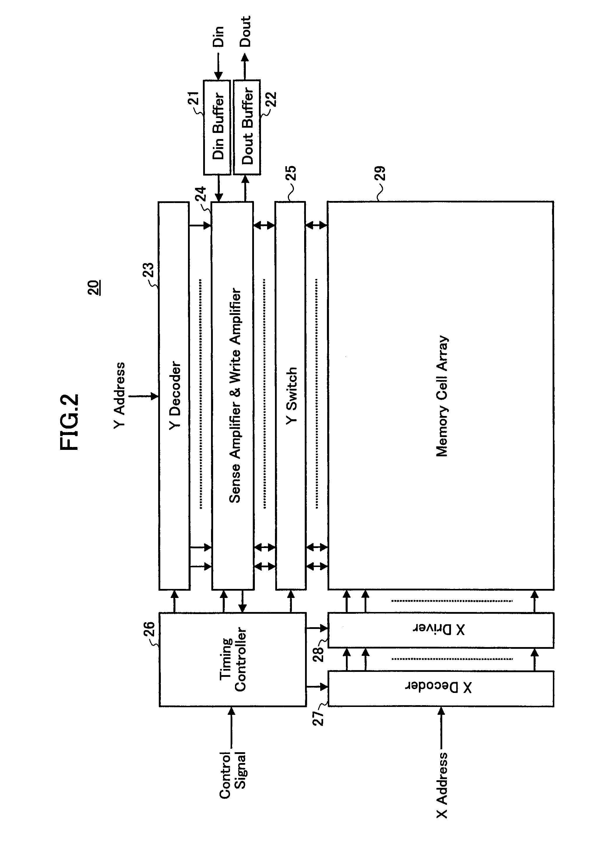
[0065]FIG. 2 is a block diagram showing the configuration of a nonvolatile semiconductor memory device according to the present invention. A semiconductor memory device 20 shown in FIG. 2 includes a Din buffer 21, a Dout buffer 22, a Y decoder 23, a write-amplifier-&-sense-amplifier unit 24, a Y switch 25, a timing controller 26, an X decoder 27, an X driver 28, and a memory cell array 29.

[0066]The memory cell array 29 includes a plurality of memory cells arranged in a matrix form, with a plurality of word lines extending in a first direction, and a plurality of bit lines extending in a second direction perpendicular to the first direction. Each memory cell has a circuit configuration as will later be described. The memory cells arranged in the same column (same Y address) are connected to the same bit lines, and the memory cells arranged in the same row (same X address) are connected to the same word line.

[0067]The timing controller 26 receives control signals from an exterior of t...

second embodiment

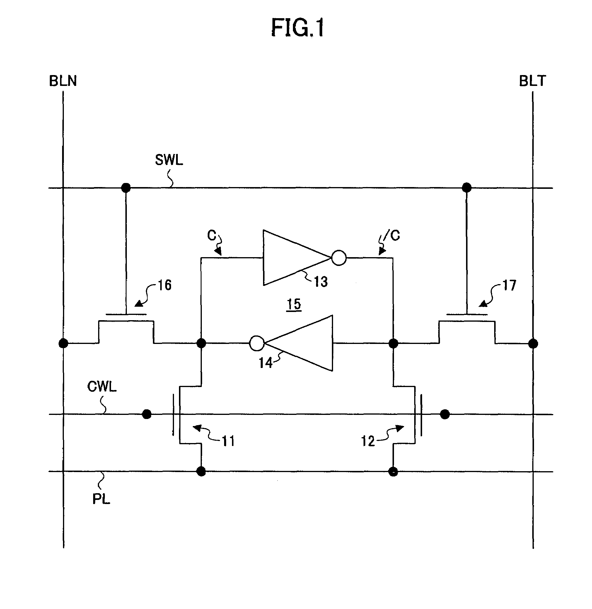
[0099]FIGS. 7A and 7B are illustrative drawings for explaining the write and store operations of the memory cell shown in FIG. 3. In FIGS. 7A and 7B, the same elements as those of FIGS. 2, 3, and 4A through 4C are referred to by the same numerals, and a description thereof will be omitted.

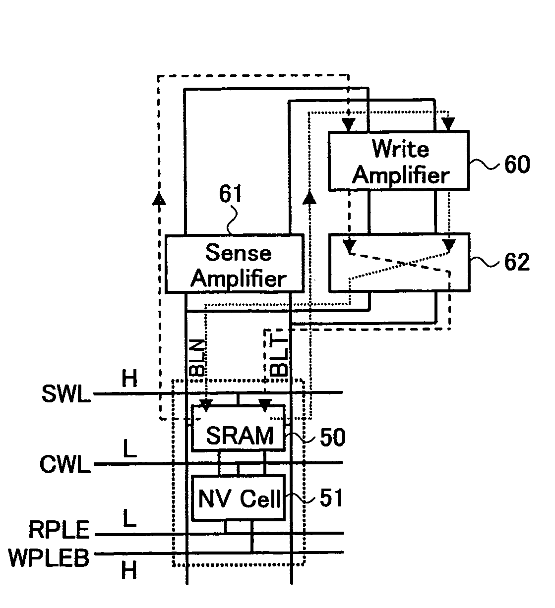
[0100]FIG. 7A shows a write operation by which data supplied from the exterior of the semiconductor memory device 20 is stored in the SRAM cell 50. As shown in FIG. 7A, the SRAM word line SWL is set to HIGH, and the NV word line CWL is set to LOW. Further, the recall plate voltage enable line RPLE is set to LOW, and the store plate voltage enable line WPLEB is set to HIGH.

[0101]With these settings of the signal lines, data is supplied from the exterior to the write buffer 60 via the Din buffer 21. The two binary values output from the write buffer 60 to the bit lines BLN and BLT are stored in the SRAM cell 50, with the SRAM word line SWL being in the HIGH state to couple the bit lines BLN and BLT t...

third embodiment

[0142]FIG. 17 is a block diagram showing the configuration of a nonvolatile semiconductor memory device according to the present invention. In FIG. 17, the same elements as those of FIG. 10 are referred to by the same numerals, and a description thereof will be omitted.

[0143]A semiconductor memory device 20B shown in FIG. 17 differs from the semiconductor memory device 20A shown in FIG. 10 in that the input into an inverting circuit (71B) shown in FIG. 17 is supplied directly from the sense amplifier unit 24-2, and that the output from the inverting circuit is supplied to the ECC check-&-correct unit 72. Such provision is made in this embodiment in order to perform the inversion of data bits and redundant bits as post-processing after a recall operation.

[0144]FIG. 18 is an illustrative drawing for explaining a store operation of the semiconductor memory device 20B. In FIG. 18, the same elements as those of FIG. 17 are referred to by the same numerals, and a description thereof will ...


PUM


Abstract

A nonvolatile semiconductor memory device includes a control circuit, an inverting circuit, and memory units, each of the memory units including a latch having a first node and a second node, a plate line, a first MIS transistor having one of source / drain nodes coupled to the first node of the latch, another one of the source / drain nodes coupled to the plate line, and a gate node coupled to a word line, and a second MIS transistor having one of source / drain nodes coupled to the second node of the latch, another one of the source / drain nodes coupled to the plate line, and a gate node coupled to the word line, wherein the control circuit is configured to invert the data latched in the latch by reading the data from the latch, causing the inverting circuit to invert the read data, and writing the inverted data to the latch.

Description

BACKGROUND OF THE INVENTION[0001]1. Field of the Invention[0002]The present invention generally relates to a memory circuit, and particularly relates to a nonvolatile memory circuit which is capable of retaining stored data in the absence of a power supply voltage.[0003]2. Description of the Related Art[0004]Nonvolatile semiconductor memory devices, which can retain stored data even when power is turned off, include flash EEPROMs employing a floating gate structure, FeRAMs employing a ferroelectric film, MRAMs employing a ferromagnetic film, etc.[0005]In the case of EEPROMs, there is a need to manufacture a transistor having a special structure comprised of a floating gate. In the case of FeRAMs and MRAMs, which achieve nonvolatile storage by use of a ferroelectric material and a ferromagnetic material, respectively, there is a need to form and process a film made of these respective materials. The need for such transistor having a special structure and the need for such film made o...

Claims


Application Information

Patent Timeline
Patent Type & Authority Patents(United States)
IPC IPC(8): G11C11/00
CPCG11C14/00G11C14/0063
Inventor KIKUCHI, TAKASHINODA, KENJI
Owner NSCORE
Why Eureka
Try Eureka