
Glass-modified stress waves for separation of ultra thin films and nanoelectronics device fabrication

a nanoelectronics and ultra thin film technology, applied in the direction of force measurement by measuring optical property variation, instruments, using mechanical means, etc., can solve the problem of generating a compressive shock wave directed towards the test coating interfa

Active Publication Date: 2009-02-10
RGT UNIV OF CALIFORNIA
View PDF8 Cites 16 Cited by
  • Summary
  • Abstract
  • Description
  • Claims
  • Application Information

AI Technical Summary

Benefits of technology

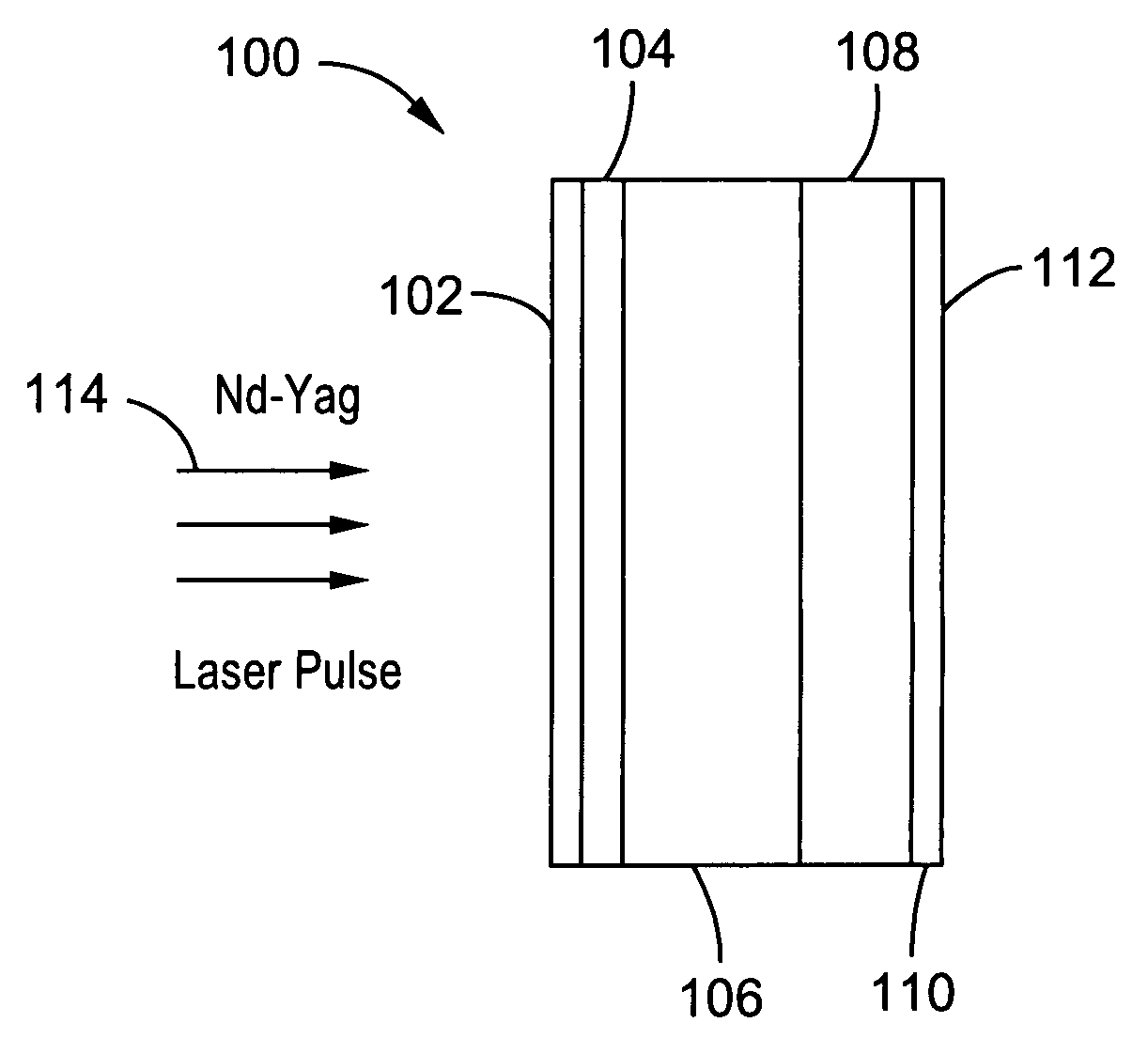
The invention is an apparatus and method for generating a tensile stress between a coating and a substrate to separate the coating from the substrate. The apparatus includes a glass element disposed on the substrate and a laser source directed at the glass element to propagate a stress wave to the coating / substrate interface to separate the coating from the substrate. The method involves positioning a glass element on the substrate and directing a laser beam at the glass element to generate a tensile stress. The invention can be used in various applications such as separating a coating from a semiconductor device or a nanostructure from a substrate.

Problems solved by technology

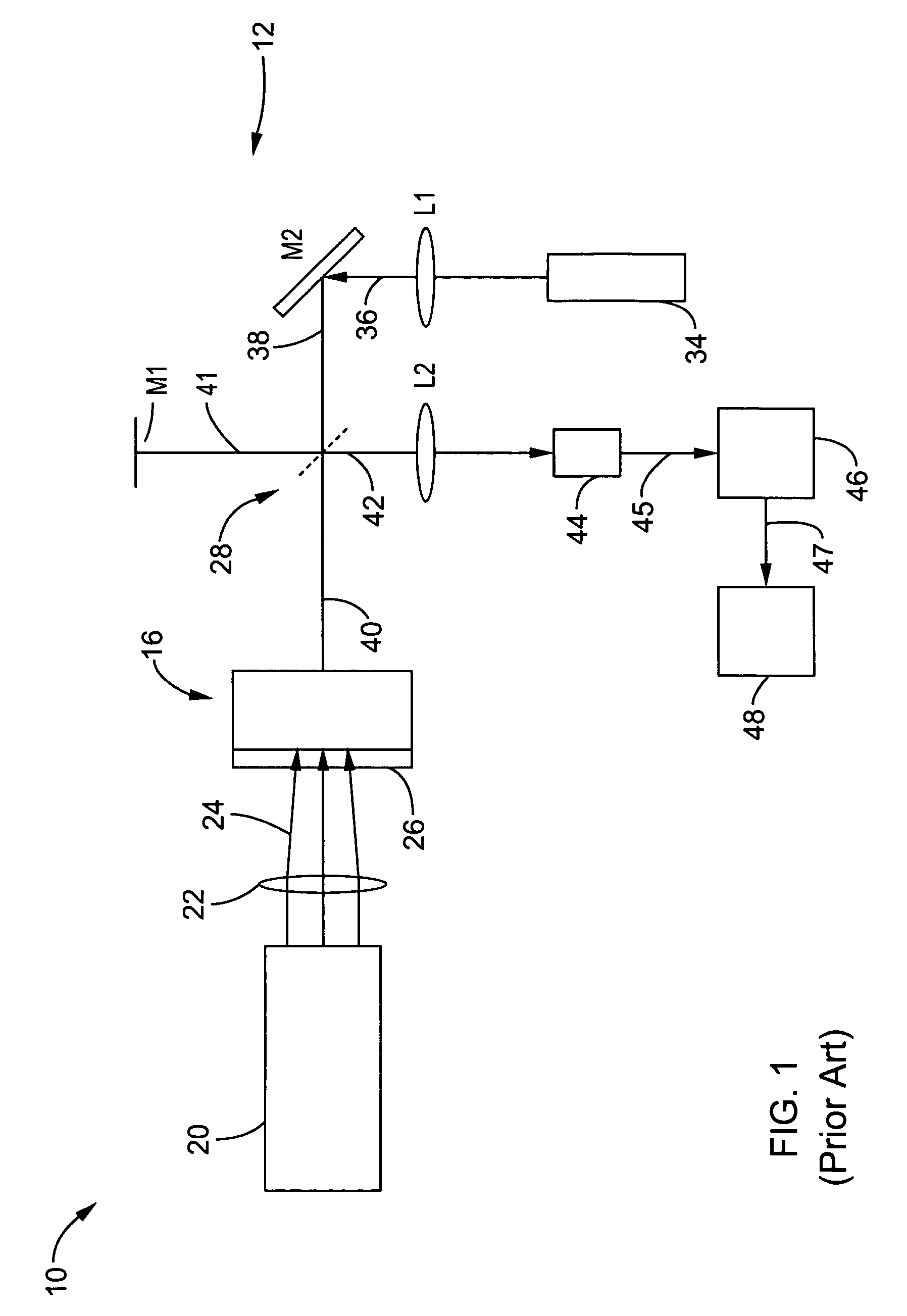
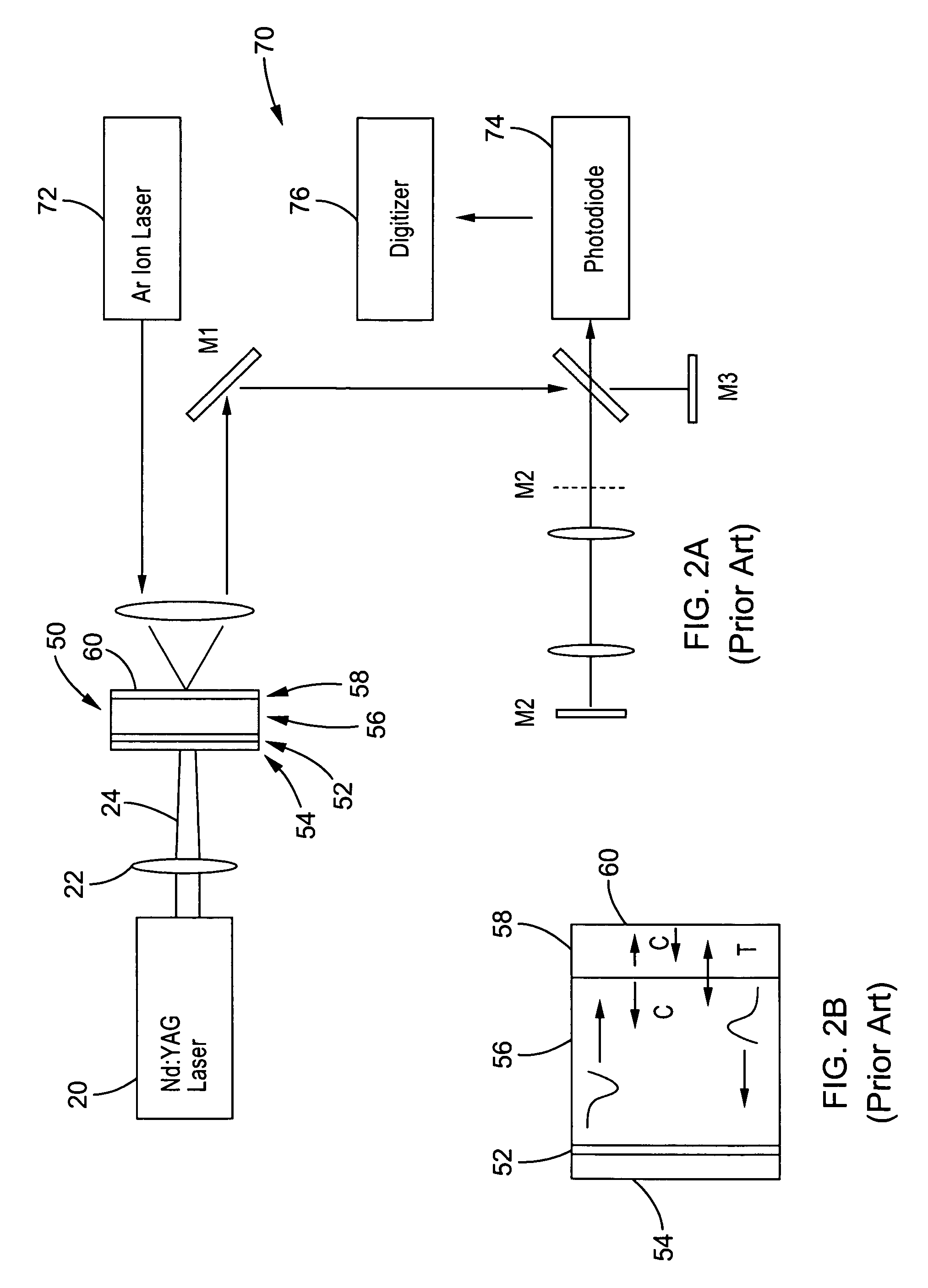
Absorption of the laser energy in the confined gold leads to a sudden expansion of the film which, due to the axial constraints of the assembly, leads to the generation of a compressive shock wave directed towards the test coating interface.

Method used


Image

  • Glass-modified stress waves for separation of ultra thin films and nanoelectronics device fabrication
  • Glass-modified stress waves for separation of ultra thin films and nanoelectronics device fabrication
  • Glass-modified stress waves for separation of ultra thin films and nanoelectronics device fabrication

Examples


Embodiment Construction

[0050]Referring more specifically to the drawings, for illustrative purposes the present invention is embodied in the apparatus generally shown in FIG. 4 through FIG. 6 and FIG. 7B through FIG. 13. It will be appreciated that the apparatus may vary as to configuration and as to details of the parts, and that the method may vary as to the specific steps and sequence, without departing from the basic concepts as disclosed herein.

[0051]The apparatus and methods of the current invention measure the tensile strength (adhesion) of very thin film interfaces (thickness less than 0.5 micrometers), and their multilayers deposited on engineering substrates. The present invention achieves separation and lift of thin film lines or their complete structures from semiconductor and engineering substrates using glass-modified stress waves. Apparatus and methods are further disclosed to catch these thin films or structures on desired substrates for reconstructing structures. This can lead to a faster...


PUM

PropertyMeasurementUnit
thicknessaaaaaaaaaa
thicknessaaaaaaaaaa
thicknessaaaaaaaaaa

Abstract

A device for generating a tensile force between a substrate and a coating, wherein the substrate has a thickness defined by a first side and a second side in a first axis, and the coating is applied to the first side of the substrate such that the coating and substrate are axially spaced along the first axis in intimate facing contact with each other to form a coating / substrate interface. The apparatus has a glass element disposed on the second side of the substrate and axially spaced along the first axis. The glass element is configured to propagate a stress wave to the coating / substrate interface to generate a tensile force between the substrate and the coating.

Description

CROSS-REFERENCE TO RELATED APPLICATIONS[0001]This application claims priority from, and is a 35 U.S.C. § 111(a) continuation of, co-pending PCT international application serial number PCT / US2005 / 007304, filed on Mar. 7, 2005, incorporated herein by reference in its entirety, which designates the U.S., which claims priority from U.S. provisional application Ser. No. 60 / 550,803 filed on Mar. 5, 2004, incorporated herein by reference in its entirety.STATEMENT REGARDING FEDERALLY SPONSORED RESEARCH OR DEVELOPMENT[0002]This invention was made with Government support under Grant No. DAAD19-00-1-0491 awarded by the Army Research Office. The Government has certain rights in this invention.INCORPORATION-BY-REFERENCE OF MATERIAL SUBMITTED ON A COMPACT DISC[0003]Not ApplicableNOTICE OF MATERIAL SUBJECT TO COPYRIGHT PROTECTION[0004]A portion of the material in this patent document is subject to copyright protection under the copyright laws of the United States and of other countries. The owner ...

Claims


Application Information

Patent Timeline
Patent Type & Authority Patents(United States)
IPC IPC(8): G01L1/24
CPCC03C17/34C03C23/0025C23C14/0005G01N19/04C03C2218/32G01N2033/0096G01N2203/001G01N2203/0055G01N2203/0282G01N33/0096G01L1/24B82Y15/00B82Y35/00
Inventor GUPTA, VIJAYKIREEV, VASSILI A
Owner RGT UNIV OF CALIFORNIA
Learn More