Assemblies and multi-chip modules including stacked semiconductor dice having centrally located, wire bonded bond pads

a technology of semiconductor dice and multi-chip modules, which is applied in the direction of semiconductor devices, semiconductor/solid-state device details, electrical apparatus, etc., can solve the problems of reducing the height of such multi-chip modules, the difficulty of real-time reducing the number of semiconductor devices that can be placed therein, and the difficulty of achieving the effect of reducing the height of the assembly

Active Publication Date: 2009-02-17
MICRON TECH INC
View PDF31 Cites 25 Cited by
  • Summary
  • Abstract
  • Description
  • Claims
  • Application Information

AI Technical Summary

Benefits of technology

[0019]In one aspect of the present invention, a semiconductor device assembly includes a first semiconductor device with a plurality of spacers arranged over an active surface thereof, a second semiconductor device positioned at least partially over the first semiconductor device, and discrete conductive elements protruding over at least a portion of the active surface, and extending through at least one common aperture formed between the spacers, the active surface of the first semiconductor die, and the back side of the second semiconductor device. The spacers are of a height that spaces the first and second semiconductor devices apart from one another by a distance substantially the same as a predetermined distance that maintains electrical isolation between the discrete conductive elements protruding over the active surface of the first semiconductor device and the back side of the second semiconductor device while minimizing the height of the assembly.

Problems solved by technology

Due to the disparity in processes that are used to form different types of semiconductor devices (e.g., the number and order of various process steps), the incorporation of different types of functionality into a single semiconductor device has proven very difficult to actually reduce to practice.
Notably, since the sizes of the semiconductor devices of such a multi-chip module must continue to decrease as they are positioned increasingly higher in the stack, the obtainable heights of such multi-chip modules and the number of semiconductor devices that may be placed therein is severely limited.
Thus, the multi-chip modules of the '060 patent may be undesirably thick due to the use of thick spacers or adhesive structures between each adjacent pair of semiconductor devices, resulting in wasted adhesive and excessive stack height.
Nonetheless, an undesirably large amount of additional space may remain between the tops of the bond wires protruding from one semiconductor device and the back side of the next higher semiconductor device of such a stacked multi-chip module.
This is a particularly undesirable limitation due to the ever-increasing feature density of state-of-the-art semiconductor devices, which is often accompanied by a subsequent need for an ever-increasing number of bond pads on semiconductor devices.
The use of such preformed spacers is somewhat undesirable since an additional alignment and assembly step is required for each such spacer.
The elongated shape of the spacer strip increases the surface area contact of the die and spacer, leading to problems from CTE mismatch.

Method used


Image

  • Assemblies and multi-chip modules including stacked semiconductor dice having centrally located, wire bonded bond pads
  • Assemblies and multi-chip modules including stacked semiconductor dice having centrally located, wire bonded bond pads
  • Assemblies and multi-chip modules including stacked semiconductor dice having centrally located, wire bonded bond pads

Examples


Embodiment Construction

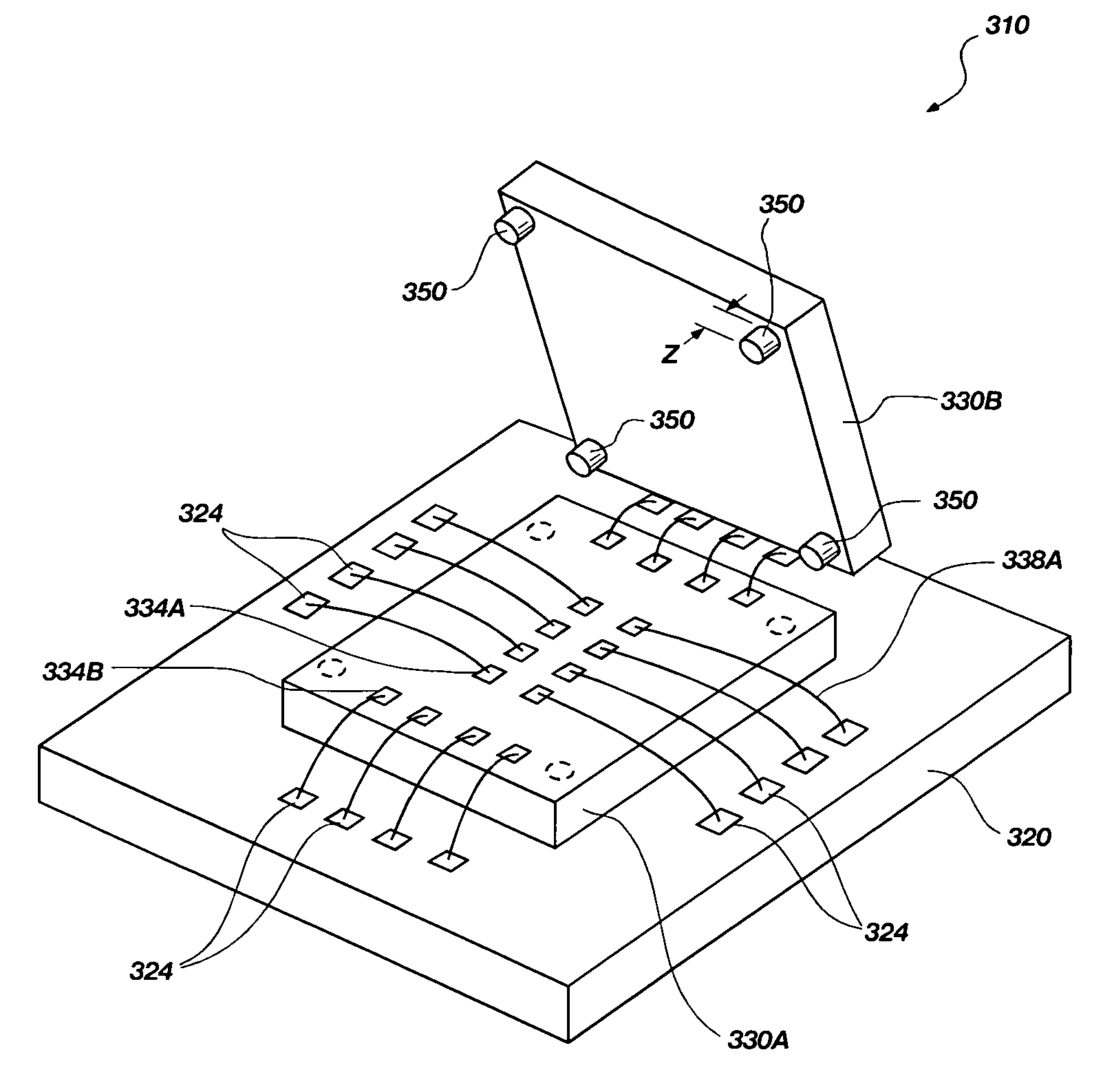
[0046]Generally, the present invention contemplates that spacers may be disposed between adjacent semiconductor devices comprising an MCM. Further, the active surfaces of both of the adjacent semiconductor devices may be oriented in substantially the same direction. Also, the semiconductor device having an active surface directly facing a back side of the adjacent semiconductor device may include centrally located bond pads that are wire bonded to a substrate. Such a configuration may provide an MCM with improved flexibility and reliability. As used herein, the term “semiconductor device” includes, for example, a semiconductor die of silicon, gallium arsenide, indium phosphide or other semiconductive material configured as a processor, logic, memory or other function, wherein integrated circuitry is fabricated on an active surface of the die while part of a wafer or other bulk semiconductor substrate that is later “singulated” to form a plurality of individual semiconductor dice.

[00...


PUM


Abstract

An assembly method that includes providing a first semiconductor device and positioning a second semiconductor device at least partially over the first semiconductor device is disclosed. Spacers space the active surface of the first semiconductor device substantially a predetermined distance apart from the back side of the second semiconductor device. Discrete conductive elements are extended between the active surface of the first semiconductor device and the substrate prior to positioning of the second semiconductor device. Intermediate portions of the discrete conductive elements pass through an aperture formed between the active surface of the first semiconductor device, the back side of the second semiconductor device, and two of the spacers positioned therebetween. Assemblies and packaged semiconductor devices that are formed in accordance with the method are also disclosed.

Description

CROSS-REFERENCE TO RELATED APPLICATION[0001]This application is a divisional of U.S. patent application Ser. No. 10 / 923,450, filed Aug. 19, 2004, now U.S. Pat. No. 7,276,790, issued Oct. 2, 2007, which claims the benefit of the filing date of Singapore Patent Application No. 200404317-1, filed Jul. 29, 2004, the entire contents of which are hereby incorporated herein by this reference.BACKGROUND OF THE INVENTION[0002]1. Field of the Invention[0003]The present invention relates generally to semiconductor device assemblies, or so-called “multi-chip modules,” and, more specifically, to multi-chip modules in which two or more semiconductor devices are stacked relative to one another. In particular, the present invention relates to stacked semiconductor device assemblies in which the distances between adjacent, stacked semiconductor devices are determined, at least in part, by a plurality of discrete spacers interposed therebetween, and discrete conductive elements protrude from a centra...

Claims


Application Information

Patent Timeline
Patent Type & Authority Patents(United States)
IPC IPC(8): H01L23/02
CPCH01L23/3128H01L25/0657H01L2224/32145H01L2224/32225H01L2924/01087H01L24/48H01L2924/15311H01L2924/1433H01L2924/14H01L2224/48091H01L2224/48227H01L2224/48471H01L2224/73265H01L2225/0651H01L2225/06575H01L2924/09701H01L2924/00014H01L2924/00H01L2924/00012H01L2924/12042H01L24/73H01L2924/181H01L2224/05553H01L2924/10161B33Y80/00B33Y10/00H01L2224/45099H01L2224/45015H01L2924/207H01L2224/02235H01L2224/4912H01L2224/06181H01L2224/10125H01L2224/06177H01L2225/06593
Inventor SENG, ERIC TAN SWEE
Owner MICRON TECH INC
Why Eureka
Try Eureka