Assemblies including stacked semiconductor devices separated a distance defined by adhesive material interposed therebetween, packages including the assemblies, and methods

a technology of adhesive materials and semiconductor devices, applied in the field of semiconductor device assemblies, can solve the problems of large amount of real estate, difficult to actually reduce the implementation of different types of functionality into a single semiconductor device, and large amount of space, so as to facilitate the introduction and spread of the effect of assembly and reducing the overall height of the assembly

Inactive Publication Date: 2005-03-22
ROUND ROCK RES LLC
View PDF11 Cites 11 Cited by
  • Summary
  • Abstract
  • Description
  • Claims
  • Application Information

AI Technical Summary

Benefits of technology

The adhesive material preferably has a viscosity that facilitates introduction thereof between the first and second semiconductor devices and, possibly, around portions of discrete conductive elements between the first and second semiconductor devices without resulting in the formation of voids therein. The wetting properties of an adhesive material may facilitate spreading thereof over the active surface of the first semiconductor device and the back side of the second semiconductor device, as well as capillary action, or “wicking” through the spaces between the first and second semiconductor devices and around the portions of

Problems solved by technology

The amount of surface area on a carrier substrate that may be saved by stacking semiconductor devices is readily apparent a stack of semiconductor devices consumes roughly the same amount of real estate on a carrier substrate as a single, horizontally oriented semiconductor device or semiconductor device package.
Due to the disparity in processes that are used to form different types of semiconductor devices (e.g., the number and order of various process steps), the incorporation of different types of functionality into a single semiconductor device has proven very difficult to actually reduce to practice.
As the sizes of the semiconductor devices of such a multi-chip module must continue to decrease as they are positioned increasingly higher on the stack, the obtainable heights of such multi-chip modules become severely limited.
Thus, the multi-chip modules of the '060 Patent may be undesirably thick due to the use of thick spacers or adhesive str

Method used


Image

  • Assemblies including stacked semiconductor devices separated a distance defined by adhesive material interposed therebetween, packages including the assemblies, and methods
  • Assemblies including stacked semiconductor devices separated a distance defined by adhesive material interposed therebetween, packages including the assemblies, and methods
  • Assemblies including stacked semiconductor devices separated a distance defined by adhesive material interposed therebetween, packages including the assemblies, and methods

Examples


Embodiment Construction

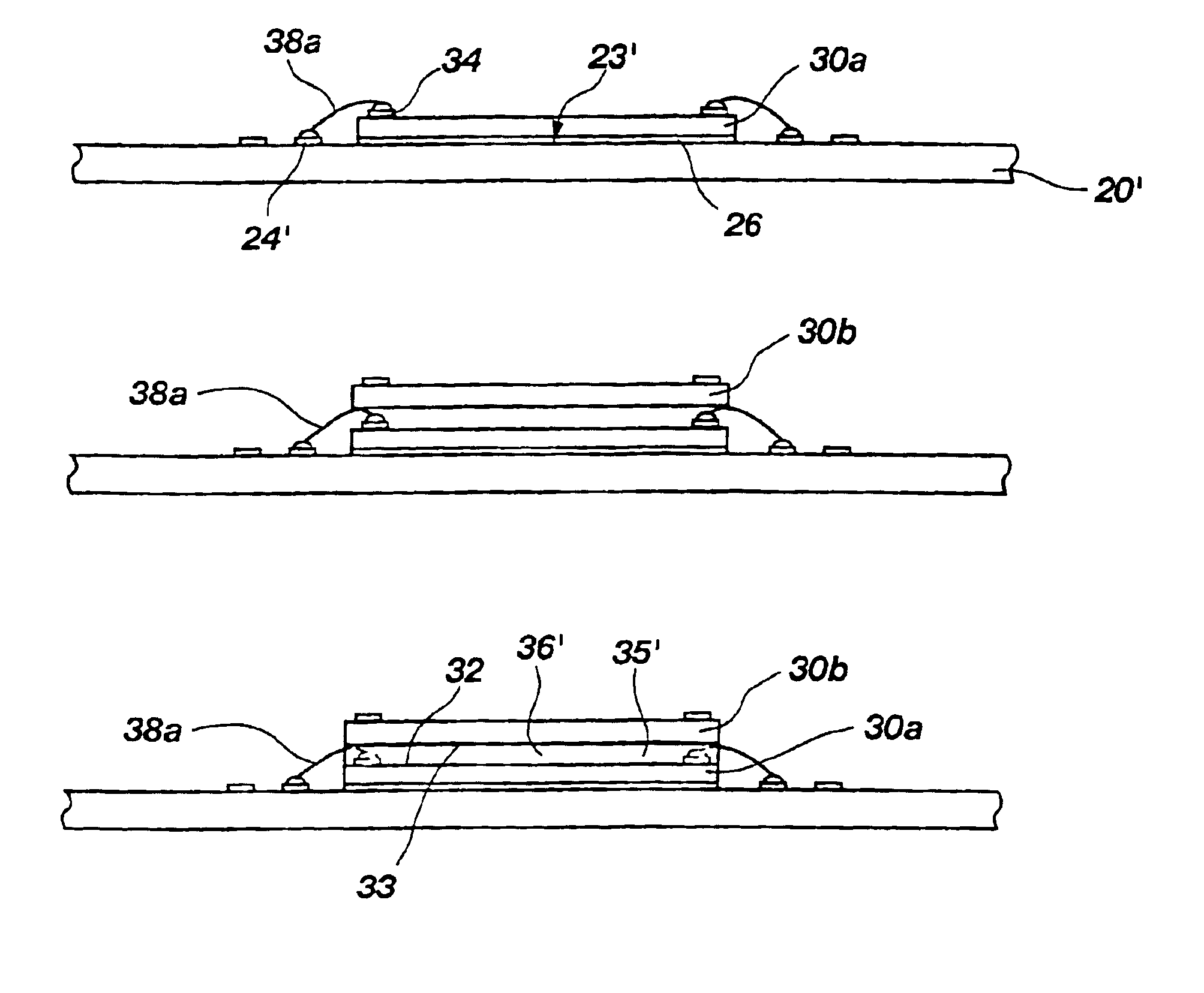
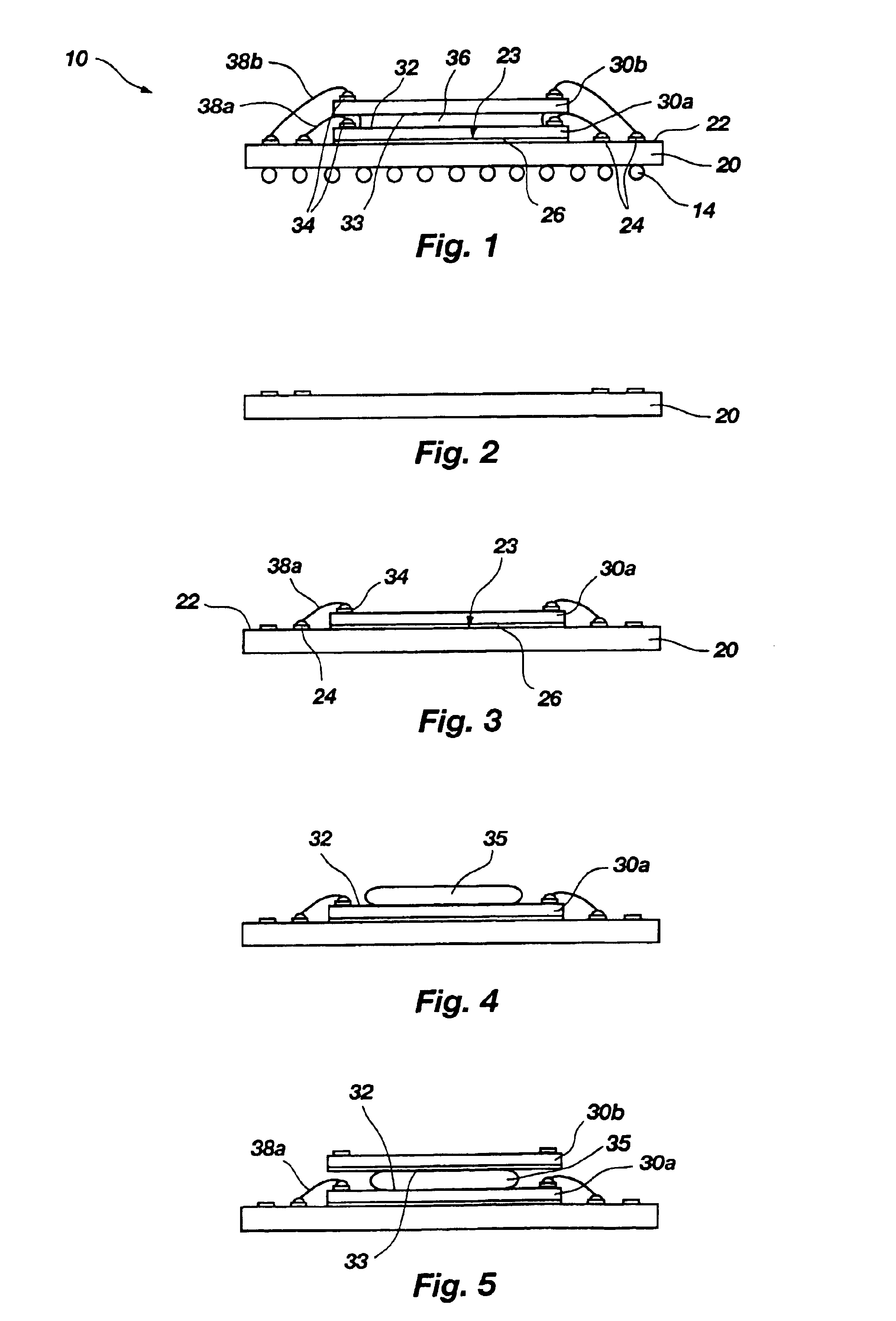
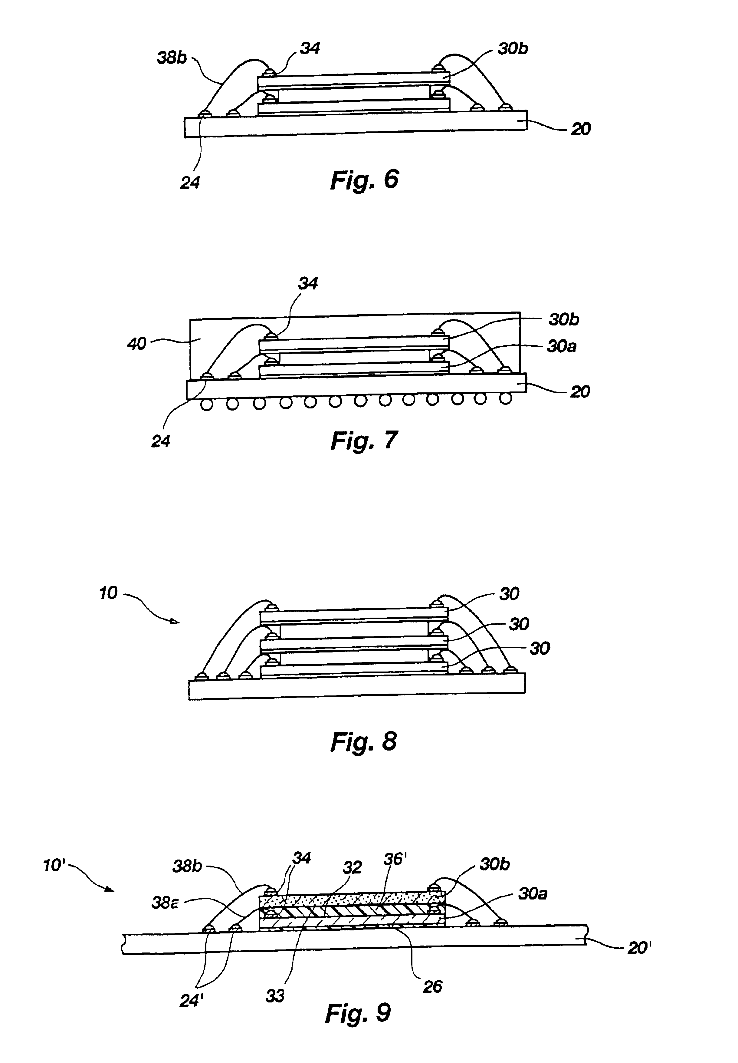
With reference to FIG. 1, an exemplary embodiment of an assembly 10 incorporating teachings of the present invention is illustrated. As shown, assembly 10 includes a substrate 20 with two semiconductor devices 30a, 30b (collectively referred to as “semiconductor devices 30”) positioned thereover in stacked arrangement.

The depicted substrate 20 is an interposer with a number of bond pads, which are referred to herein as contact areas 24, through which electrical signals are input to or output from semiconductor devices 30 carried upon or adjacent to a surface 22 of substrate 20. Each contact area 24 corresponds to a bond pad 34 on an active surface 32 of one of the semiconductor devices 30 positioned upon substrate 20.

Of course, the use of other types of substrates, such as circuit boards, semiconductor devices, leads, and the like, in assemblies and assembly methods incorporating teachings of the present invention is also within the scope of the present invention. Accordingly, a sub...


PUM


Abstract

A method for assembling semiconductor devices includes providing a first semiconductor device, applying a volume of adhesive material to at least a surface of the first semiconductor device, and positioning a second semiconductor device over the first semiconductor device and a portion of at least one discrete conductive element protruding thereabove. The adhesive material may be applied to a surface of the first semiconductor device prior to positioning the second semiconductor device thereover, or introduced between the first and second semiconductor devices. Upon curing, the predetermined volume of adhesive material spaces the first and second semiconductor devices a predetermined distance apart from one another. Additional semiconductor devices may also be added to the assembly. The first semiconductor device may be associated with a substrate. Semiconductor device assemblies and packages that are at least partially fabricated in accordance with the method are also disclosed.

Description

BACKGROUND OF THE INVENTION1. Field of the InventionThe present invention relates generally to semiconductor device assemblies, or so-called “multi-chip modules”, and, more specifically, to multi-chip modules in which two or more semiconductor devices are stacked relative to one another. In particular, the present invention relates to stacked semiconductor device assemblies in which the upper semiconductor device of an adjacent pair of semiconductor devices at least partially overlies discrete conductive elements protruding above the lower semiconductor device of the adjacent pair and the distances between adjacent, stacked semiconductor devices are determined, at least in part, by a quantity of adhesive material interposed therebetween.2. Background of Related ArtIn order to conserve the amount of surface area, or “real estate”, consumed on a carrier substrate, such as a circuit board, by semiconductor devices connected thereto, various types of increased density packages have been...

Claims


Application Information

Patent Timeline
IPC IPC(8): H01L21/70H01L25/065H01L21/98
CPCH01L25/0657H01L25/50H01L2924/00014H01L2224/48091H01L2224/48227H01L2225/0651H01L2225/06575H01L2225/06582H01L2924/09701H01L2924/15311H01L2224/92247H01L2224/32145H01L2924/01087H01L2224/73265H01L2224/32225H01L2924/00H01L2924/00012H01L2224/45099H01L24/73B33Y80/00
Inventor DERDERIAN, JAMES M.
Owner ROUND ROCK RES LLC
Why Eureka
Try Eureka